Active-pixel CMOS sensors improve their image
After initial false starts, CMOS (complementary metal oxide semiconductor) imagers are now finding their way into desktop video systems, digital still cameras, and other products. The lure of low power, self-clocking, random access, nondestructive reading, antiblooming, and radiation tolerance is proving irresistible. Additionally, all of the control functions that are normally part of the camera system or frame grabber can be implemented on chip at low cost. The only remaining issue is how to implement the new capabilities in a product that is better and less expensive than products based on traditional technologies.
Initially CMOS imagers soured many potential users when image quality didn`t meet the hype. The single biggest obstacle to implementation of early CMOS imagers was the quality of video or the signal-to-noise ratio of the imager. With each succeeding generation, however, the signal-to-noise ratio has improved. An understanding of the pixel types may help engineers select a "camera on a chip" or "Chip Camera" technology for specific applications.
First-generation CMOS imagers - Traditional imagers were separated into three categories: the photodiode, the photogate or charge-injection device (CID), and the ubiquitous charge-coupled device (CCD). All three types were in production by the early 1970s using proprietary metal oxide semiconductor (MOS) processes to optimize the wafer yield and electro-optical characteristics. All three pixel types are considered passive in that the pixel does not have the signal buffered at the pixel site. From the 1970s through the early 1990s, relatively little was accomplished in the fabrication of CMOS area arrays. Each manufacturer of imagers had a MOS process with unique characteristics that allowed the manufacturer to survive profitably. As CMOS processes became the standard the world over and digital designs with a million transistors became commonplace, it became possible to shift area-array designs to a standard CMOS process. Hence, the first-generation CMOS imagers were developed.
Passive pixel CMOS arrays were the first generation, as all three passive pixel types were ported to CMOS. Now all three passive pixel arrays could take advantage of the CMOS process and add any and all necessary timing or video-processing functions as needed. Also, major improvements in signal-to-noise ratio for photodiodes and CIDs could be made by adding an amplifier per column or per row. In the case of a CID the total charge collected in the pixel is divided by the column capacitance, when sensed (see Fig. 1). Because capacitors in parallel add, the total column capacitance is equal to the capacitance of a pixel multiplied by the number of pixels in the column. For example, if the maximum signal at the pixel collection photogate is 2 V for a 5-V process, the signal, when transferred to the sense photogate, is divided by the number of pixels in the column. If there are 500 pixels in the column the signal level is divided by 500 or is only 0.004 V when measured. The reduced signal at the end of the column is further degraded by the video bus capacitance.
In older MOS processes it was only feasible to place one amplifier per array. In a MOS process, only one type of field-effect transistor (FET) is available to design amplifiers. Therefore, the resulting MOS amplifier was much larger and consumed more power than a comparable CMOS amplifier. With smaller, lower-power CMOS amplifiers, it was now possible to place an amplifier per column to isolate one column from the rest and limit the signal degradation. Also, the amplifier per column could be an amplifier with gain to rebuild the weak signal. With an amplifier per column the whole row could be buffered and have signal conditioning all at once. In effect the video bandwidth of the video-processing chain was now at line rate, not element rate. In other words the amplifier bandwidth was kilohertz, not megahertz, further improving the signal-to-noise ratio.
The amplifier per column (or row) does help to minimize the effects of sensing the photodiode or photogate pixel signal from the periphery. CCDs don`t suffer from the same problems as photogates or photodiodes because the signal collected at the pixel site is shifted to the amplifier located at the periphery. The CCD signal remains intact until it is shifted to the amplifier, with little or no degradation. CCDs, having the lowest noise floor, have dominated the market. However, they suffer from high power consumption, fixed reading format, and exact timing requirements to operate properly. Ideally, a sensor would have the flexibility of a photodiode or photogate and provide the high-quality video of a CCD. To that end, a small buffer added to a photogate or photodiode would isolate the pixel signal from the rest of the array.
Second-generation CMOS imagers - Sensors that implement a buffer per pixel are known as active-pixel sensors and represent the second generation of CMOS imagers. Adding a buffer per pixel is as simple as adding a source follower, made from one FET, and a method of biasing the pixel site, usually by adding another FET (see Fig. 2). At first one may assume that passive pixels should have a higher fill factor than active pixels. But when it comes to interline-transfer CCDs, that isn`t the case.
In interline transfer CCDs, which dominate consumer electronics, the CCD register occupies about half of the pixel size. The other half is used to collect photon-generated charge. Depending on the process used and pixel size, active-pixel sensors can have equal or better fill factor than interline CCDs. Active-pixel sensors have all the flexibility of CIDs or photodiodes and benefit from adding all the necessary timing and video processing with signal-to-noise ratios normally associated with CCDs. However, active pixels that use source followers per pixel suffer from a relatively high level of fixed pattern noise (FPN) that is objectionable to the average viewer, if not corrected in either hardware or software.
The high level of FPN associated with active-pixel sensors that use source followers for pixel buffers is due to wafer process variations that cause slight differences in the transistor thresholds and gain characteristics. Fixed pattern noise is an offset from the video average; it makes a monitor look like a dirty window screen has been superimposed on it. There are up to three possible sources of FPN. The first is the source-follower load FET. Because there is typically only one source-follower load FET per column of pixels, the FPN is column-related. The second is the source-follower in the pixel site. The source-follower pixel FET FPN is random throughout the pixel array. The third source is dependent on the type of correlated double-sampling (CDS) circuit employed. If the CDS circuit employed uses more source-followers to buffer the video per column, then it may add more FPN on a column-by-column basis.
The same process variations that cause threshold variations per FET also cause each source-follower FET to have slightly different transconductances. The transconductance variation causes each pixel to have different source-follower gains. Each pixel has its own source follower per pixel, and source followers have less than a gain of one and typically Av = 0.86. If the gain variations per imager range an optimistic ?2% with a maximum signal level of 2 V at the pixel site, the resulting net gain change is 70 mV. This gain variation may not be part of a vendor`s stated signal-to-noise ratio. The symptom of each pixel having different gains is the dirty-window screen effect described above, which gets worse with high levels of video.
The source-follower gain variations per pixel are added to the normal gain variations that occur within each pixel, whether it is active or passive. Slight process variations that cause the above gain and threshold variations also cause slight differences, depending on how efficient each pixel is in converting photons into electrons across an imaging array.
The threshold variations that cause offsets in the video background can be almost completely eliminated with a CDS circuit, except for the third source described above. CDS circuits eliminates the pixel offsets by subtracting the background reference bias from the actual background reference of a particular pixel. The gain variation per pixel, however, cannot be easily eliminated. To properly correct for gain variations, each pixel gain would have to be stored in memory and all pixels corrected to the same gain. Due to the intensive processing of pixel-by-pixel gain correction, this solution may only be acceptable for low-bandwidth applications like still digital cameras. Another less-intensive method would be to filter (smooth) the video to minimize objectionable pixels from the viewer.
Although active-pixel sensors may have high signal-to-noise ratios, they suffer from gain variations that create objectionable (nonuniform) video. Ideally, the pixel structure would have minimal FPN and would not have gain variations from pixel to pixel. A method to eliminate the gain variations would include a full unity gain amplifier (UGA) per pixel. A UGA maintains a gain of one, by feedback from the output to the input (see Fig. 3).
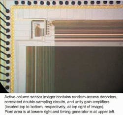
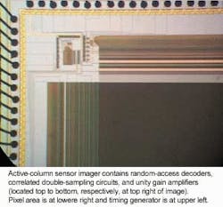
One UGA per pixel would eliminate the gain variations from pixel to pixel, but the six FETs also needed would consume most of the pixel area. However, a unity gain amplifier per pixel could be implemented if all the common FETs were located at each column and only the input signal differential FET remained at the pixel site. In effect each pixel of a selected row, via a dual-gate FET, completed a UGA per column; hence, this pixel-and-amplifier combination is called an active-column sensor (see photo on p. 111). At each column a CDS circuit eliminates video background offsets.
With the knowledge of how different CMOS pixels operate, engineers can optimize the advantageous aspects of CMOS active pixels for their applications. As always, no single imager or pixel type will serve all needs, and it is up to the designer to make the best selection for a particular purpose. o

