ORGANIC PHOTODETECTORS: Thin-film organics bring integrated optical detection to AFM probes
KWANG HYUP AN, MAX SHTEIN, and KEVIN PIPE
The use of molecular organic dyes in photodetection has many potential advantages in both large and small area device applications. Molecular organic dyes often have very large absorption coefficients (~10,000 cm-1), can be manufactured in very large quantities, and can be deposited as device-quality thin films on a variety of substrates—including metal and plastic foils, glass, and silicon—without the constraints of lattice matching, thus enabling a number of opportunities for monolithic integration.
Recently we have developed the means to fabricate organic photodetectors (OPDs) on silicon-based atomic force microscopy cantilevers for simultaneous optical and topographical imaging.1 Dual imaging of this type has many applications in biology and materials characterization and has traditionally been accomplished through near-field scanning optical microscopy (NSOM) using pulled metal-clad optical fibers. However, higher signal-to-noise ratio can be achieved by instead performing optical detection with a photodetector in close proximity to the sample. Furthermore, the spectral tuning afforded by the large library of organic compounds—such as laser dyes—and the engineering of optical microcavity effects allows much greater control over spectral response than NSOM probes fabricated with integrated III-V semiconductor devices. Finally, the use of silicon cantilevers provides much better reliability and mechanical response for topographic measurements than do pulled optical fibers or III-V-based cantilevers.
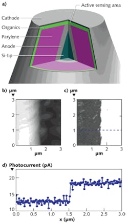
A typical OPD probe design consists of molecular organic thin films sandwiched between thin-film metallic electrodes, all deposited onto a Si AFM cantilever using vacuum thermal evaporation (see figure, part a). A thin adhesion layer, such as nickel, is first deposited onto the Si, followed by the anode (aluminum, for instance). A relatively thick parylene layer is then deposited by chemical vapor deposition, covering the entire probe surface and forming an electrically insulating film. Focused ion beam (FIB) milling is then used to define the OPD working area by cutting off the vertex of the conical tip and exposing the anode. After the subsequent deposition of the active organic layers and cathode, this exposed anode on the tip effectively defines the current collection and sensing regions. By precisely controlling the width and position of the beam during the milling step, we have formed OPDs with active areas as small as 200 nm in diameter on the probe tip.
While 200 nm spatial resolution is sufficient for many applications, we have recently explored OPD probe designs that achieve spatial resolutions significantly beyond the diffraction limit. In one realization, light from the sample passes through a nanoscale aperture in the outer metal layer at the probe/sample contact point and is waveguided a distance of about 1 μm through the parylene layer to arrive at the OPD laterally. Probes using this design have demonstrated spatial resolutions better than 60 nm under visible (λ= 475 nm) illumination (see figure, parts c and d).
Wavelength selectivity
The capability to distinguish or select different wavelengths of light can be critical for scanning probe applications, as well as for photodetection in general. While several means of achieving wavelength selectivity have been demonstrated in organic-based photodetectors, certain shortcomings remained. If a dye is selected to optimally cover a portion of the spectrum, for example, the dye must possess simultaneously appropriate electrical characteristics to produce sufficient electrical response in a photodetector, which significantly narrows (or eliminates) some material choices.
Recently, we showed a means of tuning the optical response of an organic photodetector by decoupling the photoresponse spectrum from the electrical behavior of the device using optical microcavity effects.2 In a photodetector comprising an organic heterojunction sandwiched between two metallic electrodes, these effects arise because of the interference of electromagnetic waves, as typically occurs in a dielectric cavity sandwiched by reflective layers in which the optical path length is on the order of a wavelength. Similar to a Fabry-Perot interferometer, microcavities exhibit a spectral selectivity due to resonant modes within the cavity.
The photodetector we recently demonstrated further incorporated a conductive, transparent optical spacer of molybdenum trioxide (MoO3) inside the cavity, between the organic film and one of the electrodes, placing the organic heterojunction near the peak of the resonant field. This resulted in dramatic improvements to the OPD’s spectral response: The detector sensitivity went up by two orders of magnitude over prior work, and the peak response wavelength could be tuned across a much wider range, spanning the visible spectrum. By tuning the position of the peak of optical field intensity inside the microcavity, thinner organic films could be used. Coupled with the high electrical conductivity of the MoO3 spacer layer, this enabled 15 MHz detection bandwidth.
The combination of the ability to precisely tune spectral response while retaining high bandwidth, and the achievement of 60 nm spatial resolution through near-field imaging significantly advances the state-of-the-art of organic-based photodetectors, moving them closer to more widespread application.
REFERENCES
1. K.H. An, B. O’Connor, K.P. Pipe, Y. Zhao, and M. Shtein, “Scanning optical probe microscopy with submicrometer resolution using an organic photodetector,” Appl. Phys. Lett., 93, 033311 (2008).
2. K.H. An, B. O’Connor, K.P. Pipe, and M. Shtein, “Organic photodetector with spectral response tunable across the visible spectrum by means of internal optical microcavity,” Org. Electron., 10, 1152 (2009).
Kwang Hyup An received doctoral and post-doctoral training in the Departments of Mechanical Engineering and Materials Science & Engineering, Max Shtein is a professor in the Department of Materials Science & Engineering, and Kevin Pipe is a professor in the Department of Mechanical Engineering at the University of Michigan, G.G. Brown Laboratory, 2350 Hayward, Ann Arbor, MI 48109; e-mail [email protected]; http://me.engin.umich.edu.
