Large-area avalanche photodiodes challenge PMTs
BROCK KOREN and MAREK SZAWLOWSKI
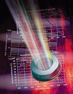
Many applications require a photodetector with the ability to quantitatively respond to low incident-light levels. Typical examples include spectrophotometers, remote sensing lidar, and medical imaging. For many years, only the photomultiplier tube (PMT) and the PIN photodiode could provide quantitative detection over the extended visible spectrum. Both technologies, however, have significant performance drawbacks. In response, the large-area avalanche photodiode (APD) was developed to deliver some of the advantages of both devices without their limitations (see photo at top of this page).
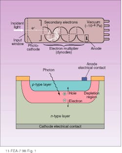
The PMT preceded the PIN photodiode and is based on vacuum tube technology. During operation an incoming photon enters the vacuum enclosure through a window and impacts a photocathode, triggering the release of an electron, which is accelerated toward another electrode (or dynode) having a positive electric potential relative to the photocathode. The electron gains energy from this acceleration, so that its impact with the dynode releases multiple secondary electrons This process is repeated through several dynodes, resulting in an overall gain of around one million at the final electrode, or anode, thus producing a measurable current from a very small incident photon flux (see Fig. 1, top).
The PIN photodiode is a semiconductor device, typically fabricated using doped silicon. In a photodiode, absorption of an incoming photon produces a single electron-hole pair. A small electric field within the photodiode causes these charge carriers to migrate in opposite directions toward external electrodes. This results in a measurable current or voltage, which has a linear relationship to the incident-light flux (see Fig. 1, bottom).The PIN photodiode is a compact, monolithic device many times smaller and lighter than the PMT. It is the low-cost detector of choice for medium- to high-light-level applications. The PMT has, however, remained the preferred detector for very-low-light applications because of its high internal gain. Although PIN photodiode signals can be electronically amplified, the noise floor of the photodiode is typically three orders of magnitude higher than that of a PMT, limiting its ability to detect low light levels.
Avalanche photodiode background
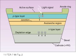
The avalanche photodiode (APD) combines the benefits of both the PIN photodiode and the PMT; it is a silicon photodiode with internal gain (see Fig. 2). As with a conventional photo diode, absorption of an incoming photon creates an electron-hole pair. A high reverse bias voltage (up to 2 kV) creates a strong internal field that accelerates the electrons through the silicon and produces secondary electrons by impact ionization. The resulting electron avalanche can produce gain factors up to several hundred.Though the design is simple in theory, the problem has always been how to fabricate a photodiode capable of withstanding the high voltage necessary for useful gain. Such a high voltage can cause massive dark noise by both bulk and surface leakage current. The bulk leakage current and subsequent damage is highly dependent on the defect density in the silicon material.
Small APDs (less than 300-µm diameter) have been commercially available for many years with gains of around 50. This small active area limited their use mostly to fiber-coupled applications. Then, in the late 1980s, the first generation of large-area devices was demonstrated in research laboratories. Volume production of practical, second-generation devices was achieved by Advanced Photonix (Camarillo, CA) in the early 1990s.
Several proprietary and patented technologies enabled successful operation of large-area APDs (LAAPDs), but the most important were the use of neutron-transmutated silicon and special passivation of the beveled edges. Instead of doping the silicon to produce an n-type layer in the conventional manner, neutron bombardment was used to transmutate some of the silicon atoms into phosphorous atoms, creating an n-type layer. Silicon prepared in this manner is characterized by excellent doping uniformity and a low number of lattice defects.
When a reverse bias is applied to a semiconductor diode, an electric field peaks at the metalurgical p-n junction. At the high operating voltages of a LAAPD, this field would normally result in edge breakdown, before a uniform avalanche breakdown can occur within the device. This problem was avoided by using a patented, beveled-edge architecture. Beveling the edge at a small angle reduced field strength at the edges of the junction.
These techniques enabled fabrication of devices up to 15 mm in diameter, with gains of several hundred and breakdown voltages of 2 kV and higher. The breakdown voltage is a very important APD parameter defining a device operating bias region for optimum performance. At voltages above breakdown, large dark current will lead to device failure through thermal runaway. On the other hand, it is important to work at voltages near breakdown, because this optimizes the ratio of gain to dark noise, that is, the signal-to-noise (S/N) ratio.
APD maturation and performance
A third-generation LAAPD delivers both superior performance and extended lifetime. Improving lifetime required fully analyzing the typical failure mechanisms and developing new processes, manufacturing methods, and lifetime testing protocols.
One specific goal was to reduce the number of defects and local inhomogeneities in the various layers, because these were identified as the leading cause of early failure. This was accomplished by reducing the overall thermal budget during device fabrication. In particular, the diffusion process used to create the gallium-doped p-type layer was eliminated, because this involved heating the substrate for an extended period of time and often resulted in a p-type layer with unacceptable uniformity. The p-type layer is now produced by a proprietary process that avoids both these limitations.
Another innovation has been to switch to lower-resistivity silicon, which lowers the breakdown voltage from 2.9 to approximately 1.9 kV. This reduces the optimum operating voltage by about 1000 V, while still delivering an avalanche gain of 300. Together, these and various other factors have enabled repeatable production of LAAPDs with extremely long lifetimes (more than 100,000 hours) and with active areas ranging from 5 to 20 mm in diameter.
Comparing LAAPDs and PMTs
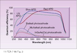
The majority of applications suitable for LAAPDs have until now relied on PMTs; the LAAPD, however, offers several advantages over PMTs. Large-area APDs have a significantly higher quantum efficiency (QE) than a PMT. Quantum efficiency is the efficiency with which light is detected. In a typical PMT, only 10%-25% of incident photons are converted into photoelectrons at the photocathode, and even this efficiency is achieved only over a narrow spectral range. In a LAAPD, the QE can be as high as 90% throughout the visible spectrum and as high as 80% at 1000 nm (see Fig. 3).The most obvious advantage of the LAAPD is that it is a rugged, compact, monolithic detector and thus is generally useful in applications where space is at a premium or where the detector may be subjected to shock or vibration. The traditional PMT is a relatively bulky, mechanically fragile glass tube, although some rugged miniature PMT devices have recently become available. Another advantage of solid-state technology is higher dynamic range. In a PMT, increases in incident light level eventually cause a cloud of electrons to build up around the anode grid. This cloud exerts a repulsive force on the other electrons coming from the final dynode, thus limiting the linear response range of a typical PMT to about four orders of magnitude. On the other hand, the LAAPD provides a linear response range up to 106.
Both PMTs and LAAPDs benefit from active cooling. Cooling a PMT lowers its dark current by lowering the amount of thermionic emission from the photocathode. Cooling a LAAPD reduces the dark current—and hence dark noise—due to thermally generated charge carriers and also lowers the breakdown voltage—by about 2V/C. Cooling the LAAPD also increases gain for a given bias, due to the temperature dependence of the electron and hole ionization rates. Consequently, a LAAPD cooled to °C can be operated at a maximum gain of 350, versus 200 at room temperature.
Less obvious advantages of the LAAPD may still be critically important in many applications. For instance, PMTs are extremely sensitive to stray magnetic fields that can perturb the path of the photoelectrons, whereas LAAPDs are insensitive to magnetic fields as high as 5 tesla. Photomultipliers also require long settling times after exposure to high light levels. Conversely, the LAAPD requires no settling time.
Many PMTs, particularly the common side-window type, exhibit poor spatial-response uniformity. This is not a problem for the latest LAAPDs. For example, the response of a 5-mm-diameter LAAPD varies by less than 4% across the central 95% of the active area. The photodetector window can also be a differentiating issue. Because it is part of the vacuum enclosure of a PMT, the window is an essential component. The hermetic packaging design of the LAAPD makes the window optional. The ability to couple light directly into the LAAPD is particularly advantageous in scintillation applications.
Photomultipliers do remain superior in one area, however—internal gain. They routinely deliver gains up to 106, whereas a cooled LAAPD can provide a gain of only 350. Photomultipliers can thus count single photons under optimum conditions, whereas LAAPDs have equivalent noise charge corresponding to 25 electrons. Indeed, the PMT is still the only detector for photon counting and ultralow-light-level applications. However, these represent less than 10% of traditional PMT applications. Most applications need a gain of only a couple of hundred, including OEM applications such as spectroscopy, laser ranging, radiation monitoring, material analysis, environmental monitoring, and medical imaging systems such as PET (positron emission tomography) scanners. At these intermediate light levels, quantum efficiency is more important than gain in determining overall performance.
Reliable LAAPDs are poised to replace PMTs in many traditional applications that do not require single-photon counting (see "Film transfer the large-area APD way"). Beyond that, their compact size, simple driving requirements, and high mechanical durability will enable entirely new applications requiring low light detection.
Brock Koren is director of sales and marketing and Marek Szawlowski is LAAPD senior project manager at Advanced Photonix, 1240 Avenida Acaso, Camarillo, CA 93012.
Film transfer the large-area APD way
Large-area APDs were recently chosen to replace PMTs in a state-of-the-art telecine (film to video conversion) system made by Cintel International Ltd. (Ware, England), which supplies such equipment to post-production houses and broadcasters throughout the world (see photo). The C-Reality system uses "flying spot" technology. A cathode ray tube (CRT) with the same aspect ratio as the film provides a fast scanning spot of nominally white light that is imaged onto the film frame using reduction optics, resulting in a 12-µm spot. Transmission of this spot through the film is recorded as three primary colors using dichroic RGB filters and three photodetectors.Graham Barber, Technical R&D Director at Cintel, says, "This is a very demanding application for photodetectors. Our system will support a range of resolutions and speeds—from standard video conversion through high-resolution scans at 2048 × 1536 resolution, with speeds up to 120 frames/second. Because of the very low light levels, we need both high QE (quantum efficiency) and internal gain, as well as high bandwidth (fast response). The large-area APD has proven to be ideal for this application, with the added benefit of excellent unit-to-unit consistency."


