HIGH-SPEED DETECTORS: Gigahertz-range detector enables improved experiments
Application-specific integrated circuits and microchannel plates were used to develop a high-speed detector with 768 channels and an overall count rate in the gigahertz range that greatly enhances spectroscope performance.
JEAN-MARIE BUSSAT AND CHUCK FADLEY
During the last 20 years, synchrotron radiation sources of vacuum ultraviolet radiation and soft and hard x-rays in the 20 to 10 keV range have achieved dramatic improvements in the photon brightness that can be delivered to a sample. With current “third-generation” sources, brightness has increased by about 104, opening up many new opportunities for materials characterization. There is, however, a growing gap between what these sources can provide and what can be detected in the final experiment, made larger still by emerging fourth-generation free-electron sources.
Photoelectron spectroscopy
A technique that exemplifies this source and detection gap is photoelectron spectroscopy (PS), an experiment that owes its first explanation to Einstein in 1905 via the photoelectric effect, but which is now a widely utilized tool for characterizing surfaces, interfaces, and nanostructures.
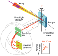
In PS, photoelectrons emitted from a sample pass into an electrostatic deflection analyzer and the various kinetic energies are imaged at different radial positions in the detection plane (see Fig. 1). The sample region and analyzer must be maintained at ultrahigh vacuum conditions. With the aid of a suitable one-dimensional imaging detector, a photoelectron spectrum can be obtained, enabling precise mapping of the electronic band structure of a sample, and revealing its chemical composition and magnetic structure. Surface atomic structure can also be determined by photoelectron diffraction and holography.
null
High-speed detection challenges
One popular detection system uses chevron-stacked microchannel plates (MCPs) for initial electron multiplication, followed by a phosphor screen inside the vacuum and a CCD camera outside the vacuum for actual counting.1 Although two-dimensional, various limitations in this system lead to acquisition times of several tens of seconds for each spectrum, and overall count-rate limits in the megahertz range. Use of the phosphor screen and CCD camera limits the counting speed and introduces nonlinearities in detector response that must be corrected. Microchannel plates can also exhibit nonlinearities, although choosing them carefully can mitigate this problem.
A much faster detector, even if only one-dimensional, would allow more rapid execution of many current experiments as well as enabling new types of time-resolved PS experiments of interest, such as tracking surface structure changes and chemical reactions in real time.
Next-generation high-speed detector
Lawrence Berkeley National Laboratory has developed an improved version of such a multichannel detector system that offers 768 channels, a maximum count rate of 2 MHz per channel (1.5 GHz overall), and a readout time as low as 500 µs.
Although the proposed system has been designed for use as an electron detector, it can easily be adapted to detect ultraviolet or visible light for laser spectroscopy applications by adding a photocathode in front of the MCP amplification stage.
Designed to replace the standard MCP pair, phosphor screen, and CCD camera, the first prototype demonstrated the feasibility of the basic design, but encountered several system-related issues including high-voltage transients and detector heating.2, 3 A newer version, described here, is based on the same architecture but involves many improvements in components and system design. Compared to related designs, the significant difference is that most of the signal-processing electronics are located inside the vacuum chamber, which reduces the number of feedthroughs, allows a greater number of channels, and via reduced noise and lower pulse counting ability, also provides much increased count rates.4
Two MCP plates in a chevron configuration are used to multiply each electron by approximately 105, with the chevron geometry preventing backscattering and afterpulsing. So-called “hot” MCPs with lower wall resistance are used to handle high count rates without saturation.
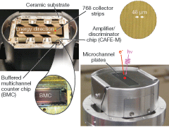
Electrons multiplied by the MCPs are measured by a linear array of 768 collector strips of chromium-gold (Cr-Au) deposited on a glass plate with a pitch of 48 µm (see Fig. 2). The electron collection area is 10 x 40 mm to match the sensitive area of the original CCD detector, which is also a typical image area in all high-performance electron spectrometers.
The signal from the collector goes to a first ASIC, the CAFE-M, which was developed originally for a high-energy physics application, and contains 128 low-noise preamplifiers and discriminators.5
Using a second specially developed signal-processing ASIC designed especially for this project, the buffered multichannel counter (BMC), the spectrum is accumulated for a preset counting time.6 This ASIC connects directly to the CAFE-M and contains 128 double-buffered counters. The double-buffered architecture allows deadtime-less operation in which the counters can be read while a new spectrum is acquired. The counters are read-out by a custom serial link operating at 40 MHz (maximum is 60 MHz). The serial-link frequency is the limiting factor in terms of readout speed and effective deadtime-less operation. A serial link was chosen because it reduces the number of through-vacuum-wall connections needed to carry information in and out of the detector. The counters have a programmable size of 8, 12, 16, or 24 bits to accommodate the needs of different experiments (smaller sizes for rapid spectral accumulation that involves signal averaging over several time scans).
In addition to the counters, the BMC contains two 8-bit digital-to-analog converters (DACs) that set the threshold and bias current of the CAFE-M. These DACs, as well as the operation of the BMC, are controlled via the serial link. The serial-link command line carries setup information to the detector. Counter content is read back via the data line. The six BMCs are daisy-chained and selected with a 4-bit address (allowing up to 16 BMCs to work together). To reduce noise coupling to the CAFE-M, the serial link uses low-voltage differential signaling (LVDS).
The collector, the six CAFE-Ms, and six BMCs are assembled on a 56 mm diameter double-sided ceramic circuit board. The ICs are directly wire-bonded on the substrate and silver epoxy glue is used to attach the passive components so as to keep outgassing of the detector low and allow smooth operation in the required ultrahigh-vacuum environment.
Outside the vacuum chamber, the detector electronics comprise a floating high-voltage power supply that biases the MCPs and provides power to the detector ICs. Detector control and data readout are accomplished with a custom data-acquisition board and a field-programmable gate array (FPGA). Because the detector is floating at high voltage, communication with the detector is accomplished by optical fiber.
First experimental results
The detector has been tested on its own with ultraviolet and electron sources and then installed on a Scienta (Uppsala, Sweden) spectrometer used at beamline 4.0.2 of the Advanced Light Source (ALS) at LBNL.7 The measured spatial resolution (full width at half maximum) of less than 3.2 channels or less than 150 µm is small enough to have a negligible effect on the energy resolution of the analyzer.
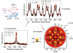
Results obtained from the ALS on a nickel oxide single crystal show that increasing the readout speed does not significantly degrade the quality of the measured spectrum or its azimuthal dependence (see Fig. 3). Photoelectron diffraction patterns and holograms can thus be obtained in much shorter times than with the original detector.
The detector linearity has also been checked at up to 1.4 MHz counting rates per channel and greatly outperforms the phosphor- and CCD-based system in this respect. Although the current Windows-based data-analysis computer represents the bottleneck in terms of data throughput and limits the readout time to 5 ms, the addition of a buffer memory in the data-acquisition interface would overcome this limitation and lead to spectral readouts in as little as 500 µs for full 24-bit accuracy.
REFERENCES
1. N. Mannella et al., J. Electron Spectroscopy and Related Phenomena 141, 45 (2004).
2. J.-M. Bussat et al., IEEE Trans. Nuclear Science 51, 2341 (2004).
3. A. W. Kay, Ph.D. Thesis, University of California, Davis, LBNL Report 46885 (September 2000).
4. L. Gori et al., Nucl. Instrum. Methods A 431, 338 (1999).
5. I. Kipnis et al., www-eng.lbl.gov/~jmbussat/ALS/CAFE-MspecV301.pdf.
6. J.-M. Bussat, various details concerning the development of this detector and the BMC ASIC are available at: www-eng.lbl.gov/~jmbussat/ALS/.
7. A. Nambu et al., J. of Electron Spectroscopy 137-140, 691 (2004).
JEAN-MARIE BUSSAT is an integrated circuit and system design engineer in the Engineering Division of the Lawrence Berkeley National Laboratory (LBNL), One Cyclotron Road, Berkeley, CA 94720. CHUCK FADLEY is a professor of physics at the University of California, Davis (UCD), One Shields Ave., Davis, CA 95616, and senior scientist in the Materials Sciences Division of the Lawrence Berkeley National Laboratory; e-mail: [email protected].


