Microscope features 300 × 300 mm automated sample stage
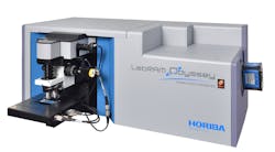
The LabRAM Odyssey Semiconductor microscope provides photoluminescence and Raman imaging on wafers up to 300 mm diameter with its 300 × 300 mm automated sample stage and its automated objective turret. A DuoScan imaging function permits both variable size laser macrospots for full wafer maps and high spatial submicron step scanning for small area maps.
Horiba Scientific
Piscataway, NJ