Hyperspectral video: The fast track to scalable solutions
Hyperspectral cameras split the light reflected by an object into many narrow spectral bands, which they capture and process separately to record a spectral signature for each pixel in a scene. This signature is much richer than the red-green-blue image that our eyes capture. It may even uniquely identify the material in the picture since each molecule interacts with light in a specific way, resulting in a spectral fingerprint.
These unique fingerprints are of excellent value for identifying and classifying all sorts of materials and objects, and are vital for further automation in industrial processes. It allows us to, for example, reveal the corrosion on the structural elements of a bridge.
The most common implementation of these cameras is called a ‘push-broom,’ which scans a scene line by line and takes several seconds or even minutes. Furthermore, these cameras are assembled by hand from many discrete components, including expensive and heavy precision optics in the glass. It requires careful alignment and calibration. These implementation factors mean only experts in hyperspectral imaging can calibrate, correct, and interpret the hyperspectral data into actual industry solutions.
Push-brooms do a great job in a conveyor-belt situation but have difficulties with a camera or scene in free movement. Think of an inspection camera in a probe robot or a free-flying drone. For these, you need to scan whole frames, preferably at video speed, to observe real-time changes. For example, when a robot takes random items out of a bin, it must take pictures permanently to make new decisions after each action. When the image gets refreshed at a rate of 30 frames per second, this results in a hyperspectral video. Today, hyperspectral video is ready to use in a wide variety of industrial contexts: quality inspection, sorting, and material detection. So how did we get there? The short answer: is chip technology.
Hyperspectral imaging on an integrated chip
Using CMOS-based infrastructure and process technology in a cleanroom, imec developed a chip with integrated hyperspectral functionality by building interference-based optical filters at the wafer level, depositing and patterning them directly on top of image sensor pixels. This approach brought important competitive advantages: the integrated imagers can be mass-produced at a cost comparable to commodity computer chips. They are also small so that they can be inserted into a regular camera with standard lenses. Such a camera is suitable for mounting a drone or a small robot.
The hyperspectral chip combines the accuracy of traditional scanning technology with increased convenience, delivering rapid refresh rates of the scene. It may scan up to 2,880 lines per second, covering the field of view with 2048 × 1088 pixels at a speed of about 30 fps in daylight conditions and up to 340 fps at higher illumination levels, as typically used in machine vision applications. The ability to fabricate extremely compact, reliable, and cost-efficient hyperspectral functionality on a chip is key to bringing this type of imaging into new markets.
Mosaic patterning technology
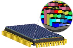
Mosaic patterning technology is used to achieve video mode hyperspectral imaging. The pixels are grouped into 3 × 3, 4 × 4, or 5 × 5 arrays. On top of each such group of, for example, 16 pixels in the 4 × 4 mosaic pattern, 16 narrow-band filters are processed, effectively making filters the size of one imager pixel (see Fig. 1). With this mosaic design, there is no longer a need for separate duplicator or beam-splitting hardware.
For industrial applications, a scientific level of data volume is not necessary. Getting the right spectral bands required for the application is key. The application specifications can be met by selecting the right image sensor with the specific speed, sensitivity, or number of pixels.
Improvements across the entire ecosystem
In addition to chip integration, collaboration across the entire value chain was needed to help close the gap between a promising technology and its application in the industry: from camera hardware manufacturers to end-users. In that context, researchers of imec partnered with Photonfocus to build lightweight and compact cameras around the integrated chips. In addition, the imec researchers validate the spectral performance of every camera, and the end-users receive direct support and software access. The result? Unprecedented system performance while significantly reducing the adoption barrier.
The youngest member of the hyperspectral camera family is Photonfocus’ 10 GigE series (see Fig. 2). These cameras allow for image data transmission at 1.1 Gbit/s and provide stronger solutions for applications requiring high bandwidth for long-distance transmission up to 100 m with a single cable. They will display their strength in fast processes such as motion analysis and virtual reality applications.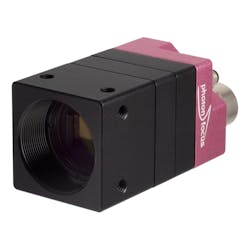
Speaking of hardware, we need to look at light. A good multispectral image starts with the proper lighting. After thoroughly examining different light sources, e.g., LED, halogen, and light bulbs, imec researchers started co-innovating with Effilux. Continuous feedback on the spectral range, power, and stability, yielded the perfect match with the integrated sensors.
At the other end of the value chain, the main challenge for the end-user was being able to interpret hyperspectral data without needing to be an expert in machine learning or hyperspectral imaging. Two software companies, perClass, and Luxflux, have built a software suite for it, elaborating on imec’s APIs, software, and the algorithms for data processing behind it, lowering the entrance barrier for hyperspectral insights.
Shortcut from problem to hyperspectral imaging solution
These improvements across the value chain have almost cut out the R&D phase for clients within the industry, closing the gap between a problem and its hyperspectral imaging solution.
Bringing together knowledge from end-users to hardware proved essential to maturing the market. New hyperspectral applications and adjacent software companies are emerging in precision farming, ecosystem protection, corrosion detection and treatment, mining, food inspection, and gas leak detection, among others. A promising technology is being put to work.
About the Author
Wouter Charle
Program Manager for Hyperspectral Imaging, imec
Wouter Charle is program manager for hyperspectral imaging at imec (Leuven, Belgium), leading off-the-shelf and evaluation system activities.