Are microLEDs the next big thing for display technology?
MicroLEDs, which are garnering a lot of attention in the display industry, could have a big impact on the photonics industry as well. Dozens of companies are developing dozens of ways to fabricate small LED devices and assemble them into displays using dozens of alternative methods. It is a richly innovative field but also a very confusing one, with no clear winning technical approach having emerged yet. This article is an attempt to paint the big picture, covering major trends and technical approaches without getting into too much detail on any one approach.
What is a microLED?
The term microLED typically refers to the size of the emitting area of the LED device. However, there is no clear industry clarity on the size that qualifies as “micro”—and the definition can vary based on the application. For example, for virtual-reality and augmented-reality (VR/AR) glasses, the desire is to have microLED elements that are smaller than 10 μm. For direct-view displays, some like the definition to be 50 or 100 μm. Above this size is a new category called miniLED; again, no clear emitter size range has been agreed to.
To make things even more confusing, many display companies are simply calling their latest very-fine-pitch display pixels “microLEDs” regardless of the size of the emitter being used. This is because for a display device, it is the pixel pitch (the space between full-color pixels) that is more important than the LED emitter size.
The most-familiar type of direct-view LED (DV-LED) display is a so-called “videowall.” These are modular displays made from a number of “cabinets,” with each cabinet composed of several “modules.” Each module in turn has red, green, and blue (RGB) LEDs mounted on a circuit substrate along with drivers and electrical interconnections.
Over the last few years, there has been a clear trend toward narrow- or fine-pitch LED video walls. These are generally defined as pixel pitches of under 1.5 mm, with the latest prototypes now at 0.4 mm. Such displays are designed for closer viewing distances. For perspective, 0.4 mm is very close to the pixel pitch on a 65 in. 4K-UHD resolution TV. As a result, major TV brands are very interested in this technology.
DV-LED displays can meet and often exceed LCD or OLED performance in terms of luminance, dynamic range, color gamut, viewing angle, black levels, and so on. The main disadvantage is price. One of the main cost drivers for DV-LED displays are the RGB LEDs. Moving to smaller LED emitters mean less LED device material is needed—a substantial cost reduction. The other major cost factor is the packaging of the LEDs and assembly onto the module circuit boards.
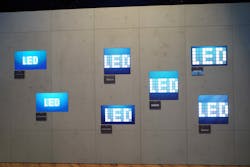
Historically, LEDs are diced from the epitaxial wafer, placed in a surface-mount package, wire-bonded in place, and encapsulated with epoxy or silicon (so-called SMD top LED). Variations in the way these LEDs are assembled on the printed circuit board (PCB) can be described as glue on board (GOB) and adhesive on board (AOB). Several newer approaches seek to reduce costs and allow smaller pixel pitches. These can be described as SMD chip LED, integrated matrix devices (IMDs), and chip on board (COB). All of these variations in device size and manufacturing approaches were demonstrated side-by-side by Lang AG (Lindlar, Germany) at the 2020 ISE trade show (February 11-14; Amsterdam, Netherlands). A photo of the small-scale demo along with a table describing the configurations and strengths/weaknesses of each are shown in Figure 1 and Table 1, respectively.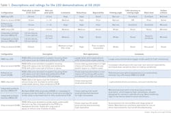
The size of the LEDs was not specified by Lang, as these can vary quite a bit (and the display makers don’t typically disclose this). However, it is likely that they are in the range of 100 to 300 μm in length or diameter, so either microLED or miniLED, depending on the microLED definition.
At ISE, AOTO (Shenzhen, China) showed a state-of-the-art 0.4-mm-pitch DV-LED microLED video wall. This is a flip-chip COB approach probably to a PCB backplane. This prototype is a single-chip solution, but AOTO says it will commercialize the 0.4 mm process soon using a multi-in-one IMD approach. The IMD package may look something as is shown in Figure 2.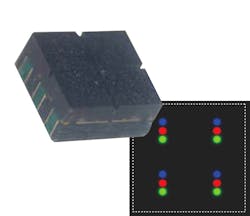
Note that the distance between each RGB set of LEDs is 0.4 mm, so the active LED diameter is around 70 μm, which is below the 100 μm microLED threshold that some use as a definition. Also note that as the active LED area gets smaller, the surrounding black area gets larger. This creates a display with a better black level and higher contrast. Sony’s Crystal LED video wall has a pixel pitch of 1.2 mm with emitters that are thought to be about 100 × 35 μm in size, leading to a display with 99% of the area being black with really great performance.
Lang AG is a company that offers display solutions to its mainly rental and staging customers. Their showcase at ISE was designed to help illustrate the difference in image quality one gets with these different packaging and manufacturing approaches. The approach Lang highlighted was the LISA display from SiliconCore (Guangzhou, China), which uses a single flip-chip approach overcoated with a thin layer of adhesive silicon and black adhesive between the flip-chip devices (see Fig. 3). This display uses microLEDs with a pixel pitch of 0.83 mm and has a luminance of 2000 nits.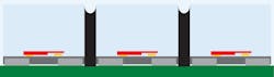
Challenges remain for all these technologies, which impacts their high costs. For example, most DV-LED displays still wire-bond the LED inside the package or to the PCB. Flip-chip devices eliminate all the wire bonding, but require that the surface of the LED epiwafer be planarized so the n and p contacts are at the same level. The device can then be flipped over to directly solder to the PCB.
Wire-bonded multi-in-one IMD devices are available today, as are single flip-chip LEDs, but they are not yet very common. IMD flip-chip devices are still only available as prototypes.
Singulating the individual die or IMD devices also has its issues, too. When a laser is used to separate the die, it can leave rough edges that reduce the black level. Overcoats of epoxy can also have thickness variations leading to variations in black level over the display. In addition, bad LEDs need to be removed and replaced in the manufacturing process, which can vary from doable to nearly impossible.
As Benjamin Valbert, Director LED & Displays at Lang AG, noted, “Each LED videowall supplier working on COB has some unique processes to optimize cost and performance parameters. The reality is that some have optimized one set of parameters and another a different set, but none have optimized all just yet. However, the fact that most of them can be solved already makes us confident for the future of COB.”
Developing next-generation microLED manufacturing
One fundamental issue with DV-LED displays is that the LED pitch on the epiwafer is very small, while the pitch on the DV-LED display can vary widely. Current mass transfer methods can transfer one to dozens of LED chips at once. To truly become cost-competitive with LCD or OLED displays, the transfer rate must increase to millions per minute. As a result, this is where a lot of innovation is concentrated now.
The most-common approach is a stamp transfer that can pick up thousands of microLEDs at a time and transfer them to a separate substrate with a different pixel pitch. Another approach uses laser pulses to transfer LEDs from a carrier substrate to the display substrate. Few details about these and other approaches are ever revealed, as they are considered proprietary intellectual property.
The next problem to worry about is yield. Not only must the mass transfer be extremely fast, but placement must be very accurate. As the size of the microLED gets smaller and smaller, the ability to pick up and accurately place it becomes more and more difficult. If a defect is found, is there a repair process that does not take far longer to complete than the initial mass transfer time? And this just applies to mechanical/electrical yield.
All the LEDs must also fall within a certain range of luminance and wavelength to provide the kind of performance demanded by end users. This is pushing the LED wafer makers to improve the way the LEDs are fabricated. New MOCVD chambers with much better uniformity and layer control are now available to enable most of the wafer to fall within quality control guidelines. Traditional gallium nitride (GaN)-based blue and green LEDs are grown on sapphire epiwafers with a 2 to 6 in. substrate size. To lower costs, larger wafer sizes are desirable. Consequently, GaN-on-silicon epiwafers are also being used to grow green and blue microLEDs at 8 in. sizes now, with the potential to go to 12 in. wafers later.
Many of these requirements point to the need to have a way to fully characterize the microLEDs at the wafer level prior to any mass transfer method. Companies are working on this need as well.
All these LEDs also need to be driven with signal to create an image. DV-LEDs mount the LEDs on a PCB and use a lot of driver chips to send signals, and next-generation DV-LEDs may well be mounted on glass substrates with active-matrix driving using TFTs at each pixel location. This will provide better control of each microLED and can leverage the TFT-on-glass fabrication infrastructure already in place for LCD displays.
Finally, since the display needs RGB LEDs, all the above improvements and techniques must be done three times for the RGB wafers.
Monolithic microLEDs
So far, we have only discussed the use of microLEDs for direct-view displays. microLEDs are also enabling very-high-density microdisplays for use in projectors, AR/VR, and head-up displays (HUDs). The main difference here is that there is no need for a mass transfer process—the on-epi pixel pitch is what is needed for these applications.
Creating full-color displays is trickier, however. For some applications like projectors and maybe HUDs, one can use three separate red, green, and blue high-density microLEDs and an x-cube combining prism to create a display, eliminating a digital-light-processing (DLP) or liquid-crystal-on-silicon (LCOS) microdisplay. Such displays should be more compact and offer higher performance than alternatives.
But for AR/VR where a single display solution is more desirable, color conversion will be needed. Here, the idea is to create high-density blue microLEDs and then pattern red and green quantum dots over two-thirds of the display. These quantum dots absorb blue light and re-emit at green or red wavelengths. Companies have already shown they can use lithography to pattern such quantum-dot materials at single-micrometer scale, so it is feasible, but many engineering challenges remain.
The backplane for these monolithic microLEDs is also different and is often CMOS silicon, as this contains the active-matrix driving circuits needed to activate the displays.
microLED performance is compelling, but costs remain high. However, there is so much activity trying to solve these engineering problems that it seems likely that the problem of high cost will be overcome in the coming years. In a decade, I predict microLEDs will be one of the most dominant display technologies, so keep your eye on this sector.
Chris Chinnock is president and owner of Insight Media, Norwalk, CT; e-mail: [email protected]; www.insightmedia.info.
About the Author
Chris Chinnock
Chris Chinnock is president and owner of Insight Media in Norwalk, CT. He is a 30-year display industry veteran with experiences in displays, broadcast, cinema, ProAV, and consumer electronics.