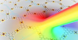
Metal-organic semiconductor photodetector has 400 to 1575 nm spectral detection range
To help satisfy the increasing demand for digital cameras and other optoelectronic components, industry is searching for new photodetecting semiconductor materials, which ideally should cover a broad range of wavelengths while being low in cost. A new hybrid material, developed at Helmholtz-Zentrum Dresden-Rossendorf (HZDR; Dresden, germany), fulfills both these requirements. Himani Arora, a physics PhD student, demonstrated that a metal-organic framework can be used as a broadband photodetector.1 As it does not contain any cost-intensive raw materials, it can be produced inexpensively in bulk.
Metal-organic frameworks (MOFs), which are highly porous substances up to 90% of which are composed of empty space, have up to now largely been used to store gases, for catalysis, or to slowly release drugs in the human body.
“The metal-organic framework compound developed at TU Dresden comprises an organic material integrated with iron ions,” says Artur Erbe, head of the Transport in Nanostructures group at HZDR’s Institute of Ion Beam Physics and Materials Research. “The special thing about it is that the framework forms superimposed layers with semiconducting properties, which makes it potentially interesting for optoelectronic applications.”
Himani Arora investigated the two-dimensional MOF semiconductor’s electronic properties; she explored, among other things, to what extent the light sensitivity was dependent on temperature and wavelength – and found that the semiconductor could detect a broad range of light wavelengths from 400 to 1575 nm. “This is the first time we have proved such a broadband photodetection for a photodetector completely based on MOF layers,” Arora Arora notes. “These are ideal properties for using the material as an active element in optoelectronic components.”
Small bandgap makes for large spectral range
The bandgap of a semiconductor is the energetic distance between the material’s valence band and the conduction band. The smaller the bandgap, the lesser the energy required to excite an electron. “As the bandgap in the material we explored is very small [0.45 eV], only very little light energy is required to induce the electricity,” says Arora. “This is the reason for the large range of the detectable spectrum.”
By cooling the detector down to lower temperatures, the performance can be improved yet further because the thermal excitation of the electrons is suppressed. Other improvements include optimizing the component configuration, producing more reliable contacts and developing the material further.
“The next step is to scale the layer thickness,” says Erbe. “In the study, 1.7 μm MOF films were used to build the photodetector. To integrate them into components, they need to be significantly thinner.” If possible, the aim is to reduce the superimposed layers to 70 nm. Down to this layer thickness, the material should exhibit comparable properties. If the group can prove that the functionality remains the same in these significantly thinner layers, they can then move to the production stage.
Source: https://www.hzdr.de/db/Cms?pNid=99&pOid=60714
REFERENCE:
1. H. Arora et al., Advanced Materials (2020); doi: 10.1002/adma.201907063.
About the Author

John Wallace
Senior Technical Editor (1998-2022)
John Wallace was with Laser Focus World for nearly 25 years, retiring in late June 2022. He obtained a bachelor's degree in mechanical engineering and physics at Rutgers University and a master's in optical engineering at the University of Rochester. Before becoming an editor, John worked as an engineer at RCA, Exxon, Eastman Kodak, and GCA Corporation.