Photonics Applied: Photovoltaics—2D ‘hot’ solar funnels increase energy flow for better photovoltaics
ADOLFO DE SANCTIS
Although the amount of energy received from the Sun in one hour could power the entire world for one year, scientists and engineers are not able to harvest and use sunlight due to the limited ability of photovoltaic (PV) solar cells to convert this energy to electricity.
The average power conversion efficiency (PCE) of commercial solar panels is currently 24% and fundamental physical limitations impose a theoretical maximum PCE of 31%. However, research conducted at the University of Exeter in England offers the possibility to build PV cells exceeding 60% PCE by exploiting a phenomenon called “inverse charge funneling”.
By applying a non-uniform strain gradient to a new class of two-dimensional (2D) semiconductors, a non-uniform change in the energy gap of charge carriers and consequent “funneling” of charges away from the strain region can enhance the responsivity of a photodetector by a staggering 350%.
Pioneering a new PV approach
In 2015, humankind consumed 20200 TWh of electricity, which translates into a total demand of 2.3 TW to satisfy the growing world population.1 This demand was met with non-renewable sources for 77%, while the remaining 23% was met by renewable sources—of which PV generation represented only 5%.
The massive use of non-renewable sources is known to have a strong effect on climate change, loss of biodiversity, environmental pollution, and ultimately physical health and quality of life.2-3 Although the amount of power received from the Sun in 1 hour equals the world energy demand, the present efficiency of solar cells—24% on average—limits the use of such an abundant power source.4
The scenario just outlined could drastically change if the efficiency of solar cells is pushed far above the current limits. However, physical limitations in the PV materials and architecture impose a theoretical maximum efficiency of 31% for single-bandgap solar cells, known as the Shockley-Queisser limit.5 The most promising, but largely unexplored, way to boost the efficiency of PV devices is the fabrication of a “hot-carrier” solar cell, which is expected to achieve a theoretical maximum efficiency of 65%.6
Essentially, hot-carrier solar cells aim to increase PV output by collecting ‘hot’ photogenerated charge carriers with high kinetic energies before those carriers lose most of their energy as heat. Unfortunately, heat is generated when a PV material absorbs photons with energy higher than the material’s bandgap. Researchers at the University of Exeter, led by Prof. Saverio Russo, demonstrated a novel technique exploiting the physical attributes of a 2D engineered semiconductor, which could overcome the aforementioned limits and enable the commercial development of these hot-carrier solar cells.7
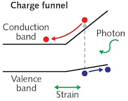
This physical phenomenon, known as “charge funneling,” allows the efficient extraction of photogenerated charges into an external circuit using a non-uniform bandgap profile in a strain-engineered semiconductor (see Fig. 1). Here, strain is used to locally modify the energy gap of a semiconductor.
A simple analogy helps explain how charge funneling can boost solar cell efficiency. If one tries to fill a bottle with a narrow neck by simply pouring liquid from a bucket, very little liquid will enter the bottle. Conversely, if a funnel is placed on top of the bottle, a much more efficient transfer of the liquid takes place. In a similar fashion, a “charge funnel” allows extraction of electrons and holes created by the incident light into a semiconducting material in a more efficient way. However, realizing such a distinct type of funnel is very challenging.
Photo-oxidation-enabled strain engineering
The first challenge is that traditional semiconductors are not suitable for realizing charge funnels. What is needed is a material in which the energy gap can be tuned along the device in a non-uniform way. One such way to tune the energy gap is to stretch the material. However, traditional semiconductors cannot sustain the large levels of strain (above 3%) necessary to achieve the funneling effect. But here is where a novel material called hafnium disulfide (HfS2) enters the picture.
A layered material akin to graphene, HfS2 is formed when single layers of sulfur and hafnium are stacked together (see Fig. 2). Most importantly, for the purposes of strain engineering, it was discovered that such a material undergoes photo-oxidation when exposed to intense laser light. Photo-oxidation occurs when a material is converted into an oxide (in this case, HfO2) when exposed to light.7
A focused laser, therefore, can be used to create a pattern in a slab of semiconductor, where a small area is oxidized. The formation of this local oxidized area induces a compression in the host material—a compression that can induce a strain gradient within the material that in turn enables the charge funneling effect.
Initial engineered samples were a few microns long, 1–2 µm wide, and 10–50 nm thick, with electrical contacts fabricated at each end by electron-beam lithography followed by gold deposition. The oxidized area was defined using a diffraction-limited laser spot (473 nm wavelength). A combination of Raman spectroscopy, spatially resolved absorption spectroscopy, and theoretical models showed that this configuration led to an average strain close to 3% in the region around the oxidized spot.
Proof of the funneling effect is revealed by scanning photocurrent maps that reveal strong photocurrent localized in the proximity of the laser-oxidized area when compared with the pristine device (see Fig. 3). Experiments to date have shown responsivity increases of up to 250%, which is extremely promising for future optoelectronic devices.
The University of Exeter has therefore demonstrated a method for creating the necessary strain gradients directly in a material without relying on complex geometrical structures fabricated on a substrate. Furthermore, for the first time, this method demonstrates what is called “inverse funneling” that allows extraction of charges away from the strain region, contrary to the “direct funneling” case that drives charges towards the middle of the strain region, making it very hard to extract them with electrical contacts.
Indeed, earlier works that probed this effect were not able to do so using electrical contacts.8 Inverse funneling truly allows the realization of new optoelectronic devices.
Photo-oxidation for high-κ dielectrics
In the field of microelectronics, photo-oxidized HfS2 has another ace up its sleeve. Advances in the manufacturing of high-quality oxide materials underpin the success of the modern microelectronic industry. As transistors shrink, the electric field density needed to modulate the flow of charges in these structures requires larger gate capacitance.
Silicon transistors have already confronted this issue, which led to the introduction of the so-called high-κ gate dielectric materials. As the dielectric constant (κ) increases, the same capacitance as silicon dioxide (SiO2) is achieved with a thinner physical layer.
In a recent publication, the team at the University of Exeter demonstrated that the oxide produced by the photo-oxidation of HfS2 can be used as a high-κ dielectric for applications in the microelectronics industry.9 A multitude of electronic devices has been demonstrated, such as flexible field-effect transistors (FETs), resistive-switching memories (ReRAM), and tunneling light-emitting diodes (LEDs) and photodetectors with performance comparable to or better than devices fabricated using traditional methods.
The use of HfS2 allows a resist-free, laser-based patterning of high-κ dielectrics and can offer multiple benefits in comparison to traditional deposition methods that rely on the use of harsh conditions involving vacuum and high-energy plasma (sputtering) or high-temperature growth in a chemically active gas environment (plasma vapor deposition and atomic-layer deposition or ALD).
These extreme growth conditions make high-κ dielectrics generally incompatible with many materials, including compound semiconductors (where high temperatures lead to the diffusion of dopants) and most flexible substrates, including textile fibers (where sputtering and ALD introduce defects). Strain-engineered HfS2 offers a solution to such problems and allows the introduction of high-κ dielectrics in the development of efficient transistors, photonic devices, wearable technologies, and for the Internet of Things (IoT).
Future research & development
Photo-oxidized HfS2 could be revolutionary for the microelectronics and solar cell industries. Not only can higher PCEs be achieved, but also new materials can be exploited that are thinner, lighter, and more flexible. Such novel semiconductor materials can do what the silicon industry cannot. Furthermore, higher efficiencies mean cleaner energy and corresponding pollution reduction for higher quality of life.
Challenges remain in the engineering of these novel materials; specifically, scaling-up the device size will require the development of large-scale growth methods for HfS2 and similar 2D layered semiconductors. By actively pursuing research to these ends, the University of Exeter is confident that it can ultimately commercialize photo-oxidized HfS2 for use in a variety of optoelectronic devices.
REFERENCES
1. See www.eia.gov/ieo.
2. J. M. Gilligan, Nat. Clim. Change, 8, 14–15 (2018).
3. J. J. Buonocore et al., Nat. Clim. Change, 6, 100–105 (2016).
4. M. A. Green et al., Prog. Photovoltaics Res. Appl., 25, 668–676 (2017).
5. W. Shockley and H. J. Queisser, J. Appl. Phys., 32, 510–519 (1961).
6. J. Nelson, The Physics of Solar Cells, Imperial College Press, London (2003).
7. A. De Sanctis et al., Nat. Commun., 9, 1652 (2018).
8. A. Castellanos-Gomez et al., Nano Lett., 13, 5361 (2013).
9. N. Peimyoo et al., Sci. Adv., 5, eaau0906 (2019).
Adolfo De Sanctis is a research fellow in the College of Engineering, Mathematics and Physical Sciences at the University of Exeter, Exeter, England; e-mail: [email protected]; https://emps.exeter.ac.uk/physics-astronomy/staff/ad642.