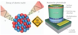
Antimonide-based SAM-APDs make sensitive gamma-ray detectors
Resulting from the radioactive decay of atomic nuclei, gamma rays can be applied in numerous applications, including astronomy, security, medical imaging, and therapy. Because gallium antimonide (GaSb) has very high absorption and efficiently stops high-energy photons due to its high atomic number, it was chosen as the absorption layer for an antimonide-based avalanche photodiode (APD) developed by researchers from the University of California, Los Angeles (UCLA) for the sensitive detection of gamma rays.
The detector is essentially a separate absorption and multiplication avalanche photodiode (SAM-APD) whereby incident high-energy gamma-ray photons are absorbed by GaSb layers (lightly p-doped, around 2 µm thick) to excite carriers that then drift into large-bandgap aluminum arsenide antimonide (AlAsSb) multiplication regions (p-i-n junctions, about 800 nm thick) and avalanche to generate internal gain with high signal-to-noise ratio.
Using a molecular-beam epitaxy (MBE) growth process for single-crystal semiconductors, the GaSb/AlAsSb heterostructures show extremely high quality and have carefully designed parameters, such as layer thickness and doping concentration, to optimize the absorption and multiplication functions of the device and eliminate the intrinsic noise. These SAM-APD gamma-ray detectors are highly sensitive: clear photopeaks are visible for americium (241Am) radioactive sources up to 59.5 keV with a minimum FWHM of 1.283 keV. This study provides the first understanding of Sb-based energy-sensitive SAM-APDs in the efficient detection of high-energy photons for gamma-ray spectroscopy. Reference: B.-C. Juang et al., Adv. Opt. Mater., 7, 11, 1900107 (Jun. 4, 2019).
About the Author

Gail Overton
Senior Editor (2004-2020)
Gail has more than 30 years of engineering, marketing, product management, and editorial experience in the photonics and optical communications industry. Before joining the staff at Laser Focus World in 2004, she held many product management and product marketing roles in the fiber-optics industry, most notably at Hughes (El Segundo, CA), GTE Labs (Waltham, MA), Corning (Corning, NY), Photon Kinetics (Beaverton, OR), and Newport Corporation (Irvine, CA). During her marketing career, Gail published articles in WDM Solutions and Sensors magazine and traveled internationally to conduct product and sales training. Gail received her BS degree in physics, with an emphasis in optics, from San Diego State University in San Diego, CA in May 1986.
