Short- and mid-wavelength infrared nanowire photodiodes are uncooled
Shortwave- and midwave-infrared (SWIR and MWIR) sensors, including focal-plane arrays (FPAs), are what enable many essential infrared sensing and imaging applications (see figure), from military (locating missiles from the heat they produce) and science (remote sensing, spectroscopy) to environmental (gas monitoring, seeing through haze). However, existing practical SWIR and MWIR sensors all suffer from a significant flaw — they require cooling. This includes sensors based on indium antimonide (InSb), mercury cadmium telluride (MCT), and indium arsenide/gallium antimonide (InAs/GaSb) type-II superlattice FPAs. The need for a cooling system adds bulk, especially to very small photodetecting systems, and raises both cost and need for maintenance.
A new approach by researchers from the University of California, Los Angeles (UCLA) and Cardiff University (Cardiff, Wales) solves this problem.1-3 The room-temperature uncooled SWIR and MWIR detectors created by the scientists consists of arrays of vertically oriented nanowires of InAs or InAsSb fabricated on an indium phosphide (InP) substrate so that the junction of the wires with the substrate creates InAs-InP heterojunctions. The structure can then be passivated with a layer of aluminum oxide (Al2O3), which lowers the nonradiative recombination at the nanowire surfaces.
Computer simulation showed that, in comparison to a planar uncooled InAs photodiode, an uncooled InAs(Sb)-InP nanowire heterojunction photodiode had a plasmonic mode resonance peak D* of 3.5 × 1010 cm Hz1/2 W-1 at a 3.0 μm wavelength—on the order of 10X higher than the planar photodiode.
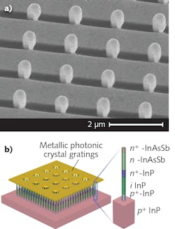
The researchers fabricated nanowire photodetectors based on a standard process that they had previously developed, growing the nanowires on patterns optimized for photodetection in the proper wavelength range, then passivating them with Al2O3. The passivation coating on the very tips of the nanowires was then removed. Using the nanowires themselves as shadow masks, gold was deposited on the nanowire-bearing surface, creating an array of nanoholes in the gold that form a plasmonic grating (see figure). This grating is important: its job is to strengthen the coupling of incident light into the nanowires’ tips via plasmonic resonances.
In an example, the fabricated active area of a SWIR device was 200 × 200 μm2. The detector surface contains nanowires with a 1300 nm pitch, 264 nm diameter, and 1650 nm height. The room-temperature spectral response for this device contains peaks at about 2.0 and 3.4 μm, corresponding to plasmonic resonances.
Next steps
Future nanowire-based IR detectors are planned that will contain photonic-crystal gratings, according to Dingkun Ren, one of the UCLA researchers. This will provide a better way to tune the peak wavelength of the devices. In the current self-assembled plasmonic structure, the plasmonic peak wavelengths are tuned by varying nanowire pitch (nanowire-to-nanowire distance). However, it is very difficult to control the growth uniformity across arrays with different nanowire pitches. In the new photonic-crystal grating structure, the peaks are engineered by varying airhole pitch, which can be simply controlled in their photolithographic fabrication. “This is a more robust optical design,” says Ren.
The group is also in the process of designing so-called separate absorption and multiplication avalanche photodiodes (SAM-APDs), which are MWIR APDs based on nanowires and metallic photonic-crystal gratings. These devices can operate in a linear mode, further increasing signal-to-noise ratio (SNR) via their internal gain. Because there is no available lattice-matched large bandgap material to make a SAM-APD structure, heteroepitaxy with large lattice-mismatches will be achieved in nanowire growth by elastically accommodating strain through nanowire sidewall facets.
REFERENCES
1. D. Ren et al., Nano Lett. (2018); https://doi.org/10.1021/acs.nanolett.8b03775.
2. D. Ren et al., Nanotechnol. (2018); https://doi.org/10.1088/1361-6528/aaed5c.
3. D. Ren et al., Nano Lett. (2019); https://doi.org/10.1021/acs.nanolett.8b04420.
About the Author
John Wallace
Senior Technical Editor (1998-2022)
John Wallace was with Laser Focus World for nearly 25 years, retiring in late June 2022. He obtained a bachelor's degree in mechanical engineering and physics at Rutgers University and a master's in optical engineering at the University of Rochester. Before becoming an editor, John worked as an engineer at RCA, Exxon, Eastman Kodak, and GCA Corporation.

