OLEDs: Reducing particle defects in cathode film layers improves OLED yield
DREW HANSER, MATTHEW GOSSEN, RICHARD BRESNAHAN, MARK O’STEEN, and SCOTT PRIDDY
Within the past decade, modern consumer electronic displays have seen great improvements in contrast ratio, pixel density, spatial resolution, and power consumption in large part because of the adoption of organic light-emitting diode (OLED) display technologies. With the ability to achieve high resolution, active-matrix OLED (AMOLED) displays are widely used in mobile consumer electronics from small wearable devices such as smart watches, to large display televisions.
To date, widespread implementation of OLED displays has been hindered by short device lifetime and high device costs resulting from low yields. Manufacturers strive to meet ever-tightening specifications, including panel-to-panel and within-panel electroluminescence uniformity. However, failure to produce panels that meet these specifications directly impacts manufacturing yield and increases production costs.
Much research has gone into drivers for improving OLED device yield, and many groups indicate that particle contamination is a major contributor to low yields. As the demand rises for larger, higher-quality, and higher-resolution OLED displays, manufacturers have had to carefully examine and control particle contamination.
Comparable to the semiconductor industry where a particle defect can ruin an entire chip, a single particle on a large OLED display can destroy the entire display. Because of the parallels of the display industry to the semiconductor industry, inspection techniques such as automated optical inspection (AOI) have been adopted from the semiconductor industry for OLED display manufactures to monitor their device yield. These AOI quality assurance systems monitor and detect electroluminescence (EL) and color consistency as well as pixel defects in each OLED display.
OLED manufacture
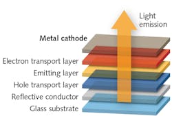
The basic structure of AMOLED devices consists of a glass substrate upon which a multilayer material stack is deposited, starting with a reflective conductive anode followed by hole transport layer (HTL), emitting layer (EML), electronic transport layer (ETL), and encapsulated with a transparent metal cathode (see Fig. 1).
Active-matrix OLED manufacturers use a vast variety of commercially available or proprietary organic materials for the HTL, EML, and ETL layers, thereby increasing the difficulty of identifying common failure modes because of the complexity and diversity of these device structures. But while each OLED manufacturer may use different organic materials, most implement a similar silver (Ag) and magnesium (Mg) alloy metal for the semi-transparent cathode layer in a top-emitting device structure. Because numerous publications have demonstrated that one failure mode of OLED devices is a direct result of pinhole and particle defects in the metal cathode, our research at Veeco Instruments focuses on reducing particle defects in this layer.1-2
The manufacturing of OLED panels is most commonly performed in large vacuum chambers. An OLED production system may be comprised of many chambers, each dedicated to a specific layer. Within the metal cathode deposition chamber, thermal evaporators—also known as effusion cells or Knudsen cells—heat high-purity Ag and Mg materials in crucibles and generate material flux plumes that are directed at a rotating or translating glass panel to carry out the deposition of a thin metal cathode film.
Today’s effusion cell solutions are adopted from the semiconductor industry, specifically from molecular beam epitaxy (MBE) component suppliers. Unfortunately, while both semiconductor and OLED applications use thermal evaporation, OLED manufacturing has vastly different process conditions than MBE, including higher deposition rates and different deposition pressures. These conditions must be considered in the effusion cell design to achieve the highest level of device quality.
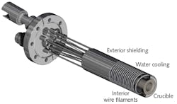
Standard MBE effusion cells use wire filaments to heat a cylindrical or conical crucible (see Fig. 2). As identified though our research and development of sources for many different types of thin-film deposition, this design does not promote the optimal flux plume required to reduce particle defects. In an attempt to improve the properties of the metal cathode film, some effusion cell suppliers have incorporated a reduced-diameter orifice insert to improve flux uniformity and impede particles from exiting the crucible. This design approach can increase particle generation, as the insert creates a colder crucible orifice that promotes material condensation, amplifying particle defects.Building upon our more than 30 years of effusion cell knowledge and development, we have leveraged proven source design technology used for other thin-film deposition applications and applied it to thermal evaporation of metals for OLED applications.
Effusion source testing for OLED cathode applications
Because of the higher deposition rates for thin-film applications, such as OLED cathodes, compared to conventional MBE rates, there are operational conditions that can result in higher particle generation when using standard thermal evaporation sources. Clearly, different source design approaches are needed.
To investigate effusion cell design strategies and their impact on the generation of particles, we experimented with several different source designs to determine the leading factors contributing to particle generation during thermal evaporation, and how best to address them. At high deposition rates, it is possible to get particles from several sources, including directly from the melt, condensation in the vapor phase, and condensation on cooler surfaces in the source. We set up a test stand to validate the source of the particles and to investigate the response of particle defects when changing effusion source design parameters.
Using a patented heater assembly to withstand the OLED operating conditions for a significantly longer period of time, we deposited films on silicon substrates at several fixed rates using different source configurations and measured particle size and distribution using optical microscopy, optical profilometry, and atomic force microscopy (AFM).
Testing results and analysis
The first experiment sought to confirm if particles were being generated directly from the melted material in the crucible. Because of the vacuum conditions for deposition, particles coming directly from the melt would primarily travel along a line of sight to the substrate. By positioning a baffle to block any line-of-sight particles from the source and comparing particle defects on the silicon substrates with and without the baffle, we did not observe a statistically significant difference between particle defect densities in either configuration and concluded that particles were not coming directly from the melt in the crucible.
We next investigated the impact of the crucible design and its configuration in the source. As discussed previously, the use of a crucible insert provides a method of modifying the flux profile from the thermal evaporation source, which may be desirable to change the deposition pattern for uniformity purposes. However, because it is a separate element in the crucible it can be cooler than the crucible itself, which can promote condensation and the generation of particles.
Veeco uses a proprietary SUMO crucible design that incorporates a reduced-diameter opening that is integrated into the crucible, enabling efficient heat transfer to the opening and reducing the likelihood of condensation while tailoring the flux profile from the source.
For the particle tests, we tested crucibles with four different diameter openings, in addition to two different crucible materials—the primary difference between the materials being the thermal conductivity of the material.
Another important part of testing the crucible design was to test the particle performance while varying the temperature gradient along the axis of the crucible. Controlling the temperature gradient allowed varying the temperature at the evaporation end (or tip) of the crucible and determining the performance impact of a cooler tip. Details of the testing results can be summarized in three main points.
First, during testing at fixed deposition rates, the temperature at the tip of the crucible was a minimum of 50°C hotter than the base of the crucible. Having a cooler tip for the crucible promotes condensation, which can be observed as droplets forming at the crucible outlet. These droplets can generate particles that are transported to the substrate as the vapor passes out of the crucible. By increasing the power to the separately controlled tip heater and increasing the temperature of the crucible outlet to the point where droplets did not form, the particle density on the substrates decreased. In addition, using a high-thermal-conductivity crucible material further reduced particle formation for the same tip temperature, highlighting the benefits of proper materials selections.
Next, testing showed that higher deposition rates at fixed tip temperatures generated higher particle counts. This occurs because higher deposition rate process conditions can lead to condensation on the tip of the crucible, which generates particles. It was possible to achieve reduced particle densities on the substrates at these higher rates by adjusting the tip to a higher temperature, as described above, demonstrating the flexible process capabilities of the source design.
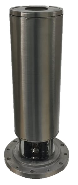
Finally, experiments demonstrated that a larger crucible opening reduced particles. A larger crucible opening has two benefits: (1) the crucible wall moves closer to the heater, improving the heating of the tip of the source; and (2) increasing the size of the opening changes the pressure of the vapor at the tip of the source and can decrease the likelihood of condensation occurring. There is a tradeoff between enlarging the opening of the crucible and affecting the desired flux profile and deposition uniformity on the substrate. Therefore, it is necessary to optimize the design of the opening for these parameters simultaneously.Through the combination of its patented heater design, SUMO crucible, crucible material selection, and flexible process capabilities, the Veeco source designed for the deposition of Ag-Mg alloy cathode films demonstrates excellent flux stability and flux profile repeatability with low particle defects for Ag and Mg evaporation, addressing the key limitations in the commercialization of OLED display technology (see Fig. 3).
REFERENCES
1. V. Madogni et al., Chem. Phys. Lett., 640, 201–214 (2015).
2. V. M. Drakonakis et al., Sol. Energy Mater. Sol. Cells, 130, 544–550 (2014).
Drew Hanser is senior director of engineering and technology, Matthew Gossen is product marketing manager, Richard Bresnahan is principal engineer, Mark O’Steen is staff scientist, and Scott Priddy is principal mechanical engineer, all at Veeco Instruments, St. Paul, MN; e-mail: [email protected]; www.veeco.com.


