METAMATERIALS/MICROSCOPY/CARDIOLOGY: Magnifying biology with metamaterials
A microscope’s focus zeroes in on a blurry looking round structure. This lysosome—a digestive organelle—measures only about 250 nm across, putting it right at the diffraction limit of resolution when using visible light. That limit might be just one optical barrier that falls away with the help of metamaterials.
Metamaterials are, literally, “beyond materials.” As explained by Purdue University metamaterials expert Alexandra Boltasseva: “We’re making artificial atoms and putting them together in a material with properties that we can’t get from nature.”
In thinking about such possibilities, Boltasseva imagines dramatically improving the resolution of a conventional light microscope with a metamaterial add-on. With such a device—some sort of novel optical material—a microscope will be able to resolve the blurry lysosome from above. It will zoom in further, maybe with 10 times higher resolution, to reveal microtubules. In the future, Boltasseva imagines seeing even more: “People with similar devices might also see smaller objects, possibly even strings of DNA,” which are only about 2.5 nm thick.
More than good as gold
Often, a metamaterial consists of metals and dielectrics. For optical applications, too much of the light gets absorbed by the traditional use of silver or gold for the metals. In her research, Boltasseva replaced the silver and gold with highly doped semiconductors to get better control over the optical properties of these metamaterials. “This opens the possibility of making tunable and switchable devices,” she says. “We can’t do this with just metals.”
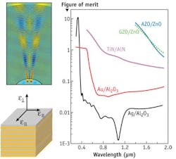
Moreover, swapping semiconductors for metals simplifies the creation of prototypes. “We can go to any industrial clean room and try to make those materials,” Boltasseva explains (see Fig. 1). Consequently, that shortens the step from simulation to realization.
Attracting illumination
Scientists need illumination to see biological structures, but too much turns destructive. “Maybe you need a light of a certain intensity and wavelength at some biological entity, like a molecule,” says University of Pennsylvania electrical engineer Nader Engheta. “You could manipulate a metamaterial to design a system to get a certain field enhancement or field confinement.”
In short, Engheta means making a nanoantenna. With metamaterials, he says, a metal surface could deliver the light and make an enhanced field at a precise point. In this way, the incoming light could be far less intense than what might be needed near the molecule of interest. “This antenna would make a local hotspot,” Engheta says.
To explain how this works, at least by analogy, Engheta talks about a guitar. “When you pluck a string, the sound waves resonate in the cavity in the body of the guitar.” Similarly, a metamaterial could include a cavity of sorts that traps light. In both the guitar and a light-trapping metamaterial, the signal gets amplified.
Theoretically, a researcher could make such a very small cavity, get light to it along a metamaterial and place the antennal part—the area where the light gets amplified—next to a biological molecule of interest. The light and the molecule would interact. For example, the light could stimulate a label on the molecule, making it visible. Maybe this system could be placed near a tumor, where it could be used as a diagnostic to see if a particular protein is being expressed.
Most important, the system could be stimulated with a low level of input light, so the signal could be seen more easily—due to lower background noise. It could also very precisely illuminate a specific area.
Random specificity
At the National Institute for Materials Science in Tsukuba, Japan, nanophotonics expert Tadaaki Nagao also explores applications of metamaterials as a sensor, using structure-controlled systems ranging from atom-scale to mesoscale. As he says, “We’ve been working on making a nanoantenna for biosensing in the mid-infrared region.”
With a metamaterial, Nagao controls the optical properties of his nanoscale sensor. Using a periodic array of identical nanoantennas, one can sense a specific molecule by tuning its resonator wavelength to that of the target molecule. In fact, he hopes to make one sensor that can detect many molecules, and he plans to do that with randomness derived from particles that are randomly shaped, sized, or distributed.
“My idea,” he says, “is that that some randomness in the metamaterials will let you detect many different molecules, because you can adjust the sensor to look at different wavelengths and you can even enlarge the bandwidth to detect unknown species.”
As a recent example, Nagao applied a single monolayer of DNA on his random antenna, and proved that a specific protein adsorbed on this DNA monolayer could be detected. The fingerprint wavelength is different for each biomolecule, but the random antenna successfully sensed many different molecules.
As Nagao says, “You need to choose appropriate adsorptive layer to bind your molecules on your sensor. And also need to do simulations to see what a specific random metamaterial would do.” (See Fig. 2.)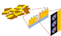
Simulating the specifics
To make the most of metamaterials, researchers need convenient ways to model them. Such modeling capabilities exist—in the form of simulation software from Lumerical Solutions (Vancouver, BC, Canada) called FDTD Solutions. But the developers didn’t start with that intention.
This company emerged from experts in photonic crystals. As explained by Lumerical’s chief technical officer James Pond, “Some of us had been doing simulations, and we thought we should write the software that we couldn’t get.”
Instead of working to address metamaterials, Pond and his colleagues aimed at broader features. They wanted flexible software that didn’t make assumptions about the geometry being simulated. Pond adds, “We also wanted software that is fast and can handle optical properties of real materials like silver and gold.” He adds, “It just so happened that we could use this to simulate all of the devices in metamaterials.”
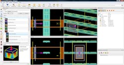
With the FDTD Solutions software, a scientist simulates a device and the transmission of light through it (see Fig. 3). “You can tune it and adjust the size of the properties and the types of materials you are using,” Pond explains.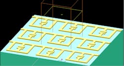
With this software, someone exploring metamaterials can simulate a range of designs and materials before making anything. “The value savings is huge,” says Pond, “because making individual prototypes is really expensive.”
With the advantage of better simulations and more ways to make new metamaterials, the advantages to biological scientists could be well worth the price.
About the Author
Mike May
Contributing Editor, BioOptics World
Mike May writes about instrumentation design and application for BioOptics World. He earned his Ph.D. in neurobiology and behavior from Cornell University and is a member of Sigma Xi: The Scientific Research Society. He has written two books and scores of articles in the field of biomedicine.