Photovoltaics: Collaboration helps scale perovskite photovoltaics for commercial deployment

DÁVID FORGÁCS
In less than a decade, perovskite photovoltaics have emerged from being merely a hyped technology in the scientific community to becoming a strong candidate for commercial implementation. Dozens of startup companies have appeared in recent years, sharing the goal of bringing this technology from the laboratory into real-life applications.
Various approaches are being explored by different entities, both in the methods used to fabricate the solar cells, as well as in their business models. There is an inherent connection between these factors, as the methods chosen will directly impact the possible materials, device architectures, performance, and the costs related to capital equipment and operational expenditures (capex and opex).
The combination of these parameters will define where the given technology will have the highest potential to penetrate the photovoltaic (PV) market, which is currently dominated by low-cost crystalline silicon cells offered by Chinese manufacturers. This stems from an oversupply, pushing down prices, that has already led to the bankruptcy of many European PV companies.
In recent years, falling costs of first-generation silicon PV products have also led to a reduction of the market share of commercially available thin-film PV devices based on cadmium telluride (CdTe) and copper indium gallium selenide (CIGS) solar cells.1 As such, the field is highly competitive, and most investors interested in emerging PV are remarkably risk-averse because of these events. It is therefore crucial for a perovskite startup to keep these elements in mind when deciding on the path to pursue in technology commercialization.
Beating or equaling silicon
As Dr. Frank Nüesch from EMPA, the Swiss Federal Laboratories for Materials Science and Technology (Dübendorf, Switzerland), said during a meeting of perovskite stakeholders held in Bern, Switzerland, there are three possible approaches that could be taken to address the market implementation of perovskite photovoltaics in such a business ecosystem: “One either marries silicon, lives next to it, or beats it.”2
From a technological perspective, the latter option is quite a challenging one for a newly emerging product. While the efficiency of perovskite solar cells has skyrocketed to the point that they outperform other commercially established thin-film PV cells at laboratory scale, there are still quite a few fundamental aspects in the physics of the material that have yet to be understood completely.
Perhaps the most crucial aspect is to understand the implications on the lifetime of perovskite solar cells, which must compete with the industrial standard of a guaranteed 25 years offered by most crystalline silicon solar module providers. Moreover, the established supply and value chain of first-generation PV puts emerging technologies at a competitive disadvantage.
This leaves two viable options. One is to combine the advantages offered by perovskite materials with existing silicon technologies, creating multijunction (also called tandem) architectures.3 Using silicon solar cells as substrates, a perovskite device can be deposited directly on top. Doing so increases the theoretical maximum efficiency of the solar cell, increasing the energy that can be harvested by such an installation on a given surface.
A hybrid option is of particular interest, considering that the costs associated directly with fabrication of a solar cell constitute only a small and steadily decreasing part of the total cost of a typical rooftop or utility-scale installation. Oxford Photovoltaics (Oxford, England) has decided to pursue this approach, which enables the company to effectively piggyback on an established technology.
While the concept sounds straightforward, there is a major challenge that must be addressed before the hybrid route can be brought to market. In a monolithic tandem solar cell, the two sub-cells that constitute the entire PV device must deliver close-to-equal performance. Otherwise, the total power output will be pinned down to the value provided by the weaker counterpart.
Complex computational methods and excellent engineering is required to optimize the layout and fabrication of such a tandem solar cell. But in fact, a perovskite/silicon tandem solar cell from Oxford Photovoltaics recently surpassed the 26.7% world-record efficiency for a single-junction solar cell, reaching 27.3% efficiency.4 This initial performance is outstanding—however, the real test will be to see how it evolves over the entire operational lifetime.
So far, perovskite solar cells have shown shorter lifetimes than silicon-based systems, and as such, the monolithic tandem approach sets extremely high expectations towards the stability of the whole solar cell stack. The deterioration of the perovskite sub-cell over time will limit the performance of the entire installation and could postpone the commercial entrance of the perovskite/silicon tandem approach.
The other option is to target market segments where silicon solar cells do not perform well. Crystalline silicon is an indirect-bandgap material, which means that incident photons need to interact with phonons to be absorbed. Because of this requirement, the chances that a photon can be harvested in low-light conditions are orders-of-magnitude less than in the case of a direct-bandgap material.
Also, the optimal thickness of silicon solar cells is in the range of around 100 μm—more than two orders of magnitude larger than the 300–1000 nm optimized thickness values of perovskite photovoltaics.5 The flexibility and significantly enhanced absorption properties of perovskites enables such ultrathin films to perform well in low-light conditions—two characteristics that are superior when compared to crystalline silicon. Harnessing these features in certain applications can therefore provide the required competitive market advantage to perovskites.
Vertical BIPV applications
Solar-energy harvesting opportunities in cities are limited because of the shortage of free horizontal areas available for traditional PV installations. There are products appearing on the market that incorporate photovoltaics in building materials, a concept referred to as building integrated photovoltaics (BIPV). With directives supporting zero-energy and carbon-neutral buildings, this market is forecast to experience rapid growth.
Solar cells can be incorporated into roofing, walls, and window materials, converting them to multifunctional energy harvesting surfaces. Crystalline silicon is being used in such applications as well—however, because of its poor low-light performance, the energy yield can be suboptimal on vertical surfaces. And while antireflective coatings can improve energy yield, overcast weather and shadowing from nearby buildings will drastically reduce crystalline silicon performance. The excellent absorption properties and flexibility of thin-film perovskite technologies allow utilization of any free area exposed to sunlight, be it direct or indirect.
Most of the companies that are aiming to commercialize the technology are indeed pursuing this path, developing solar modules that can be incorporated into building elements. But the construction industry is also very demanding, with a range of requirements and tests that must be passed to allow incorporation into structures. Architects and construction companies have their own specific needs with respect to design and quality, and it is therefore fundamental for BIPV developers to collaborate closely with their clients for successful market adaptation.
Collaborating for success
Saule Technologies strategically engages in joint development activities with its partners. The agreement signed with European construction company Skanska (Stockholm, Sweden) was the first landmark deal that was undertaken by Saule.6 In the collaboration, the teams are working together to find the most appropriate methodology to create a semitransparent perovskite solar module that will be integrated into the fenestration of office buildings. State-of-the-art laminated windows incorporate a sheet of adhesive material, typically ethylene-vinyl acetate (EVA), between two sheets of glass (see Fig. 1). This provides the structure with the safety feature of keeping the glass pieces in place in case of breakage, as well as granting additional sound barrier and ultraviolet (UV)-protection properties (see Fig. 2).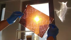

While there are plenty of advantages in the approach chosen by Saule, there are quite a few challenges. The lamination process must be compatible with the perovskite material, which is known to be both chemically and thermally sensitive. The question of stability applies here as well, as the buildings will have to stand erected for decades, and the replacement of façade elements is a very costly venture.
Because of the flexibility, light weight, and custom design of our solar modules, there are plenty of other application areas that can be explored in addition to BIPV. A few of these possibilities include automotive, apparel and wearables, portable electronics, Internet of Things (IoT), and even usage in the space industry. We are in contact with major players from these fields, jointly exploring new application opportunities. We believe that just like our solar cells, our organization must be flexible and versatile to strive in the highly competitive field of photovoltaics.
REFERENCES
1. S. Philipps and W. Warmuth, “Fraunhofer-ISE Photovoltaics Report” (Aug. 27, 2018); see https://goo.gl/U9g4pw.
2. Empa Akademie conference, Industrialization of Perovskite Thin Film Photovoltaic Technology (Oct. 2018); see https://goo.gl/xLSjq9.
3. G. E. Eperon, M. T. Hörantner, and H. J. Snaith, Nat. Rev. Chem., 1, 12, 0095 (2017).
4. See https://goo.gl/oK1xTu.
5. K. Yoshikawa et al., Nat. Energy, 2, 5, 17032 (2017).
6. See https://goo.gl/XxAJvu.
Dávid Forgács is director of knowledge management at Saule Technologies, Warsaw, Poland; e-mail: [email protected]; www.sauletech.com.