Infrared Optics: New materials extend laser spectral coverage deep into the infrared
PETER SCHUNEMANN
Interest in nonlinear optical (NLO) materials for mid-infrared (mid-IR) frequency conversion has exploded in recent years because of the emergence of new ultrafast laser applications ranging from frequency comb-based spectroscopy to high harmonic generation.
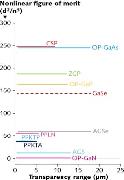
Traditional NLO oxide crystals such as lithium niobate (LiNbO3) or potassium titanyl phosphate (KTP) are limited to output wavelengths ≤5 µm because of the onset of multiphonon absorption. But NLO semiconductors such as zinc germanium phosphide (ZnGeP2 or ZGP) and, more recently, orientation-patterned gallium arsenide (OP-GaAs) offer transparency much deeper into the mid-IR region (including the terahertz range), as well as nonlinear coefficients (d values) that are 5–10X higher than those of oxides.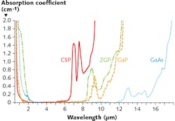
Bulk birefringent crystals: ZnGeP2 and CdSiP2
Zinc germanium phosphide (ZGP) has been the material of choice for pulsed 2 µm-pumped optical parametric oscillators (OPOs) operating between 2 and 8 µm since the first successful growth of large, low-loss, single crystals at BAE Systems led to multiwatt mid-IR OPOs in the early 1990s.1, 2 These ZGP materials have the highest thermal conductivity (35 W/mK) and (until the advent of CSP) the highest nonlinear coefficient (75 pm/V) of any bulk birefringent crystal that is transparent and phase-matchable at 2 µm.
Despite residual absorption losses at 2 µm of 0.02 to 0.05 cm-1 (arising from singly ionized Zn vacancies), extremely low losses in the 3–8 µm spectral range combined with low walk-off and minimal back-conversion enable extremely efficient NLO device operation for ZGP crystals. Development efforts in recent years have focused on increasing the yield of low-loss crystals, scaling to larger apertures, and improving laser damage threshold values.
For ZGP, aperture sizes up to 25 × 25 mm2 can be produced from standard boules and up to 30 × 30 mm2 from custom boules. Low absorption losses, improved polishing, and optimized high-temperature antireflection coatings have enabled laser damage thresholds (LDT) in excess of 4 J/cm2 (at 20 ns and 10 kHz) and enabled mid-IR (3–5 µm) average output powers approaching 100 W, as well as high-energy output exceeding 200 mJ with no obvious limits to further scaling.3, 4
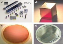
Cadmium silicon phosphide (CSP) is a new 42 m chalcopyrite analog of ZGP with a larger band gap (around 2.45 eV) and slightly larger negative birefringence that enables 1 and 1.5 µm laser pumping. This CSP material also exhibits an even-higher nonlinear coefficient: d36 = 84.5 pm/V, which is the largest of any new phase-matchable inorganic crystal in the last four decades.5
In addition, CSP can be noncritically phase-matched (NCPM) under 1064 nm pumping to generate temperature-tunable output around 6.2 µm.6 This NCPM operation also enables continuous-wave (CW) OPO operation in CSP (which has never been achieved in ZGP). Because CSP also exhibits significantly lower absorption losses than ZGP at 2 µm (>3X lower), it is an attractive alternative to ZGP for power scaling 2 µm-pumped OPOs.
Unfortunately, CSP presents some significant crystal growth challenges compared to ZGP (twinning, cracking, high growth temperature, and pressure) that currently limit the size and yield of high-optical quality crystals, but progress continues on this front.
Quasi-phase-matched semiconductors: OP-GaAs and OP-GaP
The advent of the first practical quasi-phase-matched (QPM) material—periodically poled lithium niobate (PPLN)—represented a new paradigm in nonlinear optical (NLO) materials development. No longer constrained by the strict requirements of birefringence phase matching, QPM enabled the use of a much broader range of materials, provided that a mechanism existed for creating the alternating QPM domain structure.
In ferroelectric oxides, this was achieved by applying lithographic electrodes followed by electric-field poling of periodic domains of alternating polarity. Quasi-phase matching offered the advantages of noncritical phase matching, polarization flexibility, and easily engineered functionality such as parallel or serial grating structures for tunability or cascaded nonlinear processes, respectively, as well as chirped structures for bandwidth control.
Lithium niobate, lithium tantalate, and KTP and its analogs are the primary periodically poled oxide crystals, but their performance is limited chiefly to the visible and near-IR regions because of severe multiphonon absorption losses beyond 4 µm. Semiconductors, however, are transparent far deeper into the mid-IR than their oxide counterparts, are free of the photorefractive effects that plague ferroelectrics, and offer many other outstanding properties, including much higher nonlinear coefficients, much higher thermal conductivities, higher purity levels, and very low losses when grown from the vapor phase.
Both OP-GaAs and OP-GaP are QPM nonlinear optical semiconductors grown by a novel all-epitaxial process (see Fig. 4). First, polar-on-nonpolar molecular beam epitaxy (MBE) is used to produce a GaAs (GaP) film with an orientation that is inverted with respect to the substrate. The inverted layer is photolithographically patterned and etched with the desired grating structure, and both orientations are then re-grown by hydride vapor phase epitaxy (HVPE) at rates up to 200 µm/hr to produce thick (>1 mm), low-loss (<0.01 cm-1) QPM layers for in-plane laser pumping.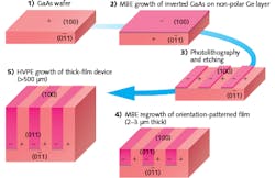
Among all QPM materials, OP-GaAs has the highest gain (d14 = 94 pm/V) and can be pumped at 2 µm to generate output at 8–12 µm and beyond, whereas OP-GaP is a low-loss QPM ZGP analog that can be pumped with 1 and 1.5 µm lasers. The more mature of these QPM semiconductors, OP-GaAs, has demonstrated >5 W of CW OPO output, whereas high-repetition-rate pulsed operation has exceeded 18 W average power output in the 3–5 m spectral range.
High-average-power experiments based on OP-GaP are still under development, but numerous OP-GaP device demonstrations have been achieved, including the first nanosecond 1 µm-pumped OPO, a broadly tunable (5–11 µm) femtosecond fiber-pumped difference frequency generator (DFG), a 1 µm-pumped femtosecond OPO (also tunable from 5 to 11 µm), a 2.6–4.2 µm frequency comb based on a 1.5 µm-pumped femtosecond OP-GaP OPO, and finally a 2.09 µm-pumped half-harmonic OPO generating 220 mW with a slope efficiency of 58%.7-11
In addition to a large indirect band gap that eliminates multiphoton absorption beyond 1 µm, bulk OP-GaP grown by HVPE exhibits highly parallel grating propagation that promises to extend aperture sizes well beyond 1 mm.
Emerging materials
In the search for new materials, two new mid-IR NLO materials—barium thiogallate (BaGa4S7) and barium sellenogallate (BaGa4Se7)—have emerged in recent years that exhibit notably wide band gaps (3.54 and 2.64 eV, respectively), deep IR transparency (cutoff at 13.7 and 18 µm, respectively), moderately high nonlinear coefficients (5 and 20 pm/V, respectively), and favorable crystal growth from stoichiometric melts.12
The fact that these low-loss crystals can be grown in large aperture sizes, exhibit reasonably high damage thresholds, and can be pumped by ubiquitous 1 µm laser sources to produce phase-matched output beyond 12 µm makes them compelling candidates for many applications. BAE Systems is currently optimizing the crystal growth and processing of BaGa4S7 and BaGa4Se7 to provide a commercial source for these rare but highly promising crystals.
Future directions
Our team at BAE Systems is committed to continued development of new and improved NLO crystals for the mid-IR region. In addition to the crystals already described, we are also beginning work on a proprietary new bulk birefringent crystal—currently referred to as LWX—that has attractive properties very similar to those of ZGP, but offers extended transparency and phase matching out to 12 µm before the onset of any significant multiphonon absorption losses.
In terms of new QPM semiconductors, we have set our sights on orientation-patterned zinc selenide (OP-ZnSe). Polycrystalline ZnSe is of course widely used for optical components in the mid-IR because of its very low absorption losses, incredibly wide transparency range (0.4–22 µm), and its commercial availability in large volumes. For QPM frequency conversion, ZnSe has the added advantages of a large nonlinear FOM (d2/n3 is approximately 200) and low dispersion that translates into large QPM grating periods to facilitate scaling to large apertures.
Unfortunately, OP-ZnSe cannot be grown by the same all-epitaxial processing approach used for OP-GaAs and OP-GaP because single-crystal ZnSe substrates are not available for processing the patterned templates and ZnSe is not readily compatible with HVPE to produce thick layers. However, ZnSe is lattice-matched to GaAs, and preliminary efforts to produce QPM ZnSe using vapor growth of ZnSe on QPM OP-GaAs templates looks promising.
While these exciting new materials are being investigated, the full potential of the best existing mid-IR NLO crystals available is yet to be realized.
REFERENCES
1. P. G. Schunemann and T. M. Pollak, “Method for growing crystals,” U.S. Patent No. 5,611,856 (Mar. 18, 1997).
2. P. A. Budni et al., “Efficient, high average power optical parametric oscillator using ZnGeP2,” Proc. ASSL, NC12, Santa Fe, NM (1992).
3. M. W. Haakestad et al., Opt. Express, 22, 7, 8556–8564 (2014).
4. A. Hemming et al., Opt. Express, 21, 8, 10062–10069 (2013).
5. V. Petrov et al., “The nonlinear coefficient d36 of CdSiP2,” Proc. SPIE, 7197-21, 1–8 (2009).
6. S. Chaitanya Kumar et al., J. Opt. Soc. Am. B, 33, D44–D56 (2016).
7. L. A. Pomeranz et al., “1064-nm-pumped mid-infrared optical parametric oscillator based on orientation-patterned gallium phosphide (OP-GaP),” Proc. CLEO_SI, SW3O.4, San Jose, CA (2015).
8. K. F. Lee et al., “Broadly tunable difference frequency generation in orientation-patterned gallium phosphide,” Proc. High-Brightness Sources and Light-Driven Interactions, JT3A.4, Long Beach, CA (2016).
9. L. Maidment et al., Opt. Lett., 41, 18, 4261–4264 (2016).
10. Q. Ru et al., “Femtosecond OPO based on orientation-patterned gallium phosphide (OP-GaP),” Proc. CLEO_SI, STu1Q.6, San Jose, CA (2016).
11. E. Sorokin et al., “Three-optical-cycle frequency comb centered around 4.2 µm using OP-GaP-based half-harmonic generation,” OSA Technical Digest (online), MS3C.2 (2016); https://doi.org/10.1364/mics.2016.ms3c.2.
12. V. Badikov et al., Phys. Status Solidi RRL, 1–3 (2010); doi:10.1002/pssr.201004425.
Peter Schunemann is chief crystal growth scientist at BAE Systems, Nashua, NH; e-mail: [email protected]; www.baesystems.com/crystals.