Topological-insulator lasers are more efficient than their contemporary counterparts
In 2012, Laser Focus World described the essential ingredients of a topological insulator—then explained as a “new state of quantum matter … [that] conducts electricity only on its surface while its interior remains insulating, an unexpected property with unknown potential for fundamental research and practical applications.” In that story, atom-thick layers of bismuth and selenium were stacked into a material that was being explored as an infrared-transparent, conductive electrode for photovoltaic cells. Six years later, researchers at the Technion – Israel Institute of Technology (Haifa, Israel), in collaboration with researchers at the University of Central Florida (Orlando, FL), have extended the science through theory and experiments by demonstrating a topological-insulator laser that is significantly more efficient than today’s semiconductor laser designs.
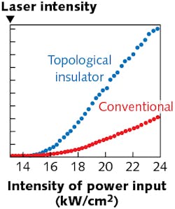
The laser consists of a two-dimensional (2D) nonmagnetic lattice of microresonators that, when pumped with light or electrical energy at the outer edge of the lattice, ferry photons easily around the perimeter before escaping as a single-mode lasing beam at one corner. Unlike other lasers that depend on flawless fabrication methods, the topological insulator laser still allows photons to flow even in the presence of lattice defects, which have little effect on the overall efficiency of the device. The laser is now being explored for use in quantum communications and silicon photonics/integrated optoelectronics networks. References: G. Harari et al., Science, doi:10.1126/science.aar4003 and M. Bandres et al., Science, doi:10.1126/science.aar4005 (both published Feb. 1, 2018).
About the Author

Gail Overton
Senior Editor (2004-2020)
Gail has more than 30 years of engineering, marketing, product management, and editorial experience in the photonics and optical communications industry. Before joining the staff at Laser Focus World in 2004, she held many product management and product marketing roles in the fiber-optics industry, most notably at Hughes (El Segundo, CA), GTE Labs (Waltham, MA), Corning (Corning, NY), Photon Kinetics (Beaverton, OR), and Newport Corporation (Irvine, CA). During her marketing career, Gail published articles in WDM Solutions and Sensors magazine and traveled internationally to conduct product and sales training. Gail received her BS degree in physics, with an emphasis in optics, from San Diego State University in San Diego, CA in May 1986.