Technology Review: Laser Focus World's top 20 photonics technology picks for 2017
The digital revolution is changing our world in ways both social and technological. While the various overt and subtle changes to our culture(s) may not be fully understood for decades, if that, the changes in technology are more straightforwardly apparent. Optics and photonics contribute hugely to the digital revolution and are in turn furthered by it. Some of these contributions are evident to the average tech-savvy but nonspecialist consumer, while others are known mainly to those in the optics and photonics arena. This year's Tech Review Top 20 list contains items from both categories.
Big-news photonics
1. Virtual and augmented reality (VR/AR). Virtual-reality headsets display a computer-simulated world, while AR glasses overlay computer-generated elements onto the real world. Are VR and AR what we'll all use in the future, or are they just toys for geeks? Actually, they're both. For example, those who want to very precisely 3D-scan a physical object into VR, perhaps to modify it in VR and then send it to a 3D printer, can do this via an interferometric scanner developed at the University of Dayton (Dayton, OH). (See "Virtual Reality Technology: Digital holographic tomography creates true 3D virtual reality," September 2017 issue; https://goo.gl/3TmdQ2.)
2. Lidar for autonomous vehicles. The idea that cars can be driven by sensor-aided computers rather than people may be disconcerting to some and a relief to others. The reality is that a well-implemented autonomous-vehicle scheme will reduce traffic jams, as well as death and injury from accidents. Crucial to this concept is sensing, with lidar as a leading candidate. Engineers at Hamamatsu (Bridgewater, NJ) are developing not only lidar systems, but sensor-fusion capabilities to integrate lidar with radar. (See "Lidar: A photonics guide to the autonomous vehicle market," November 2017 issue; https://goo.gl/XZ1ry2.)
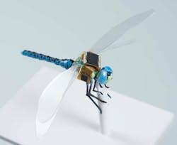
3. Light-guided cyborgs. While turning a human into an externally guided robot may be unlawful for now, turning insects into cyborgs is apparently totally legit. Researchers at The Charles Stark Draper Laboratory (Cambridge, MA) and Howard Hughes Medical Institute (HHMI; Chevy Chase, MD) have flown a dragonfly equipped with solar-powered sensors (see Fig. 1). Soon, similar dragonflies will be remotely steered via an optogenetic implant that will activate steering neurons in the insect's brain. (See "Dragonfly backpack turns insect into optogenetically steered drone," September 2017 issue; https://goo.gl/bN4eFA.)
4. LIGO honorees. As the Laser Focus World audience knows from last year's Top 20 Tech Review, the Laser Interferometer Gravitational-Wave Observatory (LIGO) has detected cosmological gravitational waves for the first time, chronicling a merger of two black holes. Since then, the European Virgo instrument has come online and, with LIGO, pinpointed a merger of neutron stars. This year, three scientists—Rainer Weiss, Barry C. Barish, and Kip S. Thorne—won the 2017 Nobel Prize in Physics for their work on LIGO and Virgo. (See "LIGO scientists receive 2017 Nobel Prize in Physics," Laser Focus World online [October 3, 2017]; https://goo.gl/1AvLt6.)
Photonics tech for us specialists
5. Ti:sapphire laser pumped with blue laser diodes. Widely used for research and increasingly for other applications, the titanium sapphire (Ti:sapphire) laser is conventionally a rather complex beast, pumped with diode-pumped solid-state (DPSS) lasers that have themselves been frequency-doubled. KMLabs (Boulder, CO) has been working on direct diode-pumped Ti:sapphire lasers that demonstrate high performance (see Fig. 2)—now, the company has introduced a compact, no-fuss commercial version. (See "KMLabs commercially introduces direct diode-pumped Ti:sapphire ultrafast laser," Laser Focus World online [September 25, 2017]; https://goo.gl/oxhe48.)6. Spherically curved CMOS arrays. A camera is not compact if its optics are large. Imaging optics usually become much bulkier and more complex when they have to be designed to focus on a flat field—for example, a CMOS or CCD array—rather than an inwardly curved field. But CMOS and CCD detectors are flat, you say? Well, that's not always true anymore: Researchers at Microsoft (Redmond, WA) and research-and-development laboratory HRL Laboratories (Malibu, CA) are creating relatively deeply curved CMOS sensor arrays by applying pneumatic pressure to flat arrays to push them into a curved substrate, then gluing them in place. (See "Spherically curved CMOS array improves image quality across the field," July 2017 issue; https://goo.gl/dkEPjh.)
7. Terahertz radiation from water. Terahertz radiation is useful for security, data communications, scientific imaging, and other applications. It is not yet a mature technology: new terahertz sources and detectors are being invented by the truckload (okay, a slight exaggeration). However, nobody has ever invented a way of generating terahertz radiation from water, at least until now. This year, an international group of researchers described the application of femtosecond laser pulses on water to achieve this feat—which could, yes, lead to a practical terahertz source. (See "Terahertz Sources: Femtosecond laser pulses produce ultrafast terahertz radiation from water," October 2017 issue; https://goo.gl/r2ytG1.)
Industrial photonics
8. Laser-assisted diamond turning. For many transmissive infrared optical materials, as well as metal optics, diamond turning is the optics fabrication method of choice because of its straightforward, deterministic nature. But how can one improve on this process? Engineers at Micro-LAM (Portage, MI) are now using a very narrow laser beam to heat and soften the optical material just before it meets the diamond tool-the process enables previously difficult-to-machine materials such as silicon to be effectively diamond-turned. (See "IR Optics Manufacturing: Laser-assisted μ-LAM process cuts through infrared optics," August 2017 issue; https://goo.gl/mDQe5V.)
9. Rapid laser materials deposition. For many types of metal components, hard chrome plating is essential to minimize wear and corrosion. The conventional laser-assisted chrome-plating process, however, is slow and wasteful of chromium—a problem, as chromium is poisonous. Researchers at Fraunhofer ILT and RWTH Aachen University (both in Aachen, Germany) have sped the chrome-plating process up by a factor of 100 while requiring far less chromium-this was achieved by having the laser melt the chromium powder particles before they fall into the melt pool on the part, rather than leaving solid particles to melt in the pool. (See "Laser material deposition gets 100 times faster," Laser Focus World online [June 1, 2017]; https://goo.gl/et2jSQ.)
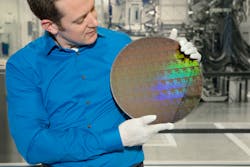
10. EUV lithography reaches 5 nm semiconductor node. Optical lithography is what defines the features found on all silicon computer chips. The leading-edge extreme-ultraviolet (EUV) lithography, under development for many years, is now trying to find its position in the march toward smaller computer-chip features dictated by Moore's Law. Some think conventional deep-UV lithography can be extended far enough to make EUV irrelevant. IBM (Albany, NY) doesn't think so, however. In fact, IBM, along with its Research Alliance partners GLOBALFOUNDRIES, Samsung, and equipment suppliers, has developed a process to build silicon nanosheet transistors that will enable 5 nm semiconductor chips (see Fig. 3), potentially leading to 30 billion transistors on a single chip. (See "IBM uses EUV lithography to reach 5 nm semiconductor node," Laser Focus World online [June 20, 2017]; https://goo.gl/1Hq4tD.)11. Erasable gratings for silicon-photonics testing. Already in wide use for communications, silicon photonics has the potential to benefit areas from science and medicine to computing and artificial intelligence (AI). However, testing of integrated silicon photonics devices and circuits is a delicate procedure if physical probes are used. If gratings are used to incouple and outcouple light, the gratings can only be placed at the input and output of the circuit, which only allows testing of the entire circuit at once. Now, researchers at the University of Southampton (Southampton, England) have learned how to fabricate erasable gratings to allow testing at any point in the circuit—the gratings are then erased via laser annealing. (See "Silicon Photonics: Erasable gratings facilitate automated PIC testing," June 2017 issue; https://goo.gl/qFc7wz.)
Biophotonics
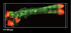
12. Bone CLARITY. Biological tissue is dense and absorbing, making imaging through tissue difficult—bone, being completely opaque, is even worse. A technique called CLARITY, in which opaque tissue components are replaced by polymer hydrogels, has been used to image, for example, deep into brain tissue at high resolution. Now, CLARITY has been further developed by researchers at the California Institute of Technology (Caltech; Pasadena, CA) and Amgen (Thousand Oaks, CA) to image through bone by making it transparent (see Fig. 4), allowing identification of cells that are progenitors of osteoporosis. (See "Intact Tissue Imaging/Light-sheet Microscopy: Clearing of intact bone promises insight into hard tissue," June 2017 issue; https://goo.gl/4HBmQa.)13. Hydrogel optical fibers. Glass and conventional polymer optical fibers, which can guide light to and from a specimen and are thus optimum in many ways for sensing, are, unfortunately, far too rigid for many biological sensing applications. However, scientists at the Massachusetts Institute of Technology (MIT) and Harvard Medical School (both in Cambridge, MA) have created optical sensing fibers consisting of a hydrogel core and a polymer cladding that can be stretched and deeply flexed and potentially implanted into biological tissue. (See "Hydrogel fibers could be used as mechanical and biochemical sensors," September 2017 issue; https://goo.gl/r252oP.)
14. Carbon monoxide lasers for surgery. The carbon dioxide (CO2) laser has been a mainstay in laser surgery ever since this type of laser was medically qualified decades ago. However, if a laser as simple and reliable as the 10.6-μm-emitting CO2 laser, but with a somewhat shorter wavelength, could be developed, then fiber transmission of the laser light would be easier, and penetration into biological tissue would be improved as well. In fact, the carbon monoxide (CO) laser, which emits at 5.5 μm, fits the bill quite well. Researchers at Art Photonics (Berlin, Germany) are experimenting with CO lasers developed by Coherent (Santa Clara, CA) for this purpose-a comparison of the two laser types used for laser tissue cutting shows that the CO laser produces a wider and deeper coagulation zone, helping to prevent bleeding. (See "Medical Lasers: Carbon monoxide laser shows surgical potential," August 2017 issue; https://goo.gl/W2f36i.)
15. Adaptive optics for in vivo subcellular imaging. Superresolution microscopy has stimulated a revolution in the biosciences—including neuroscience, where researchers wish to do imaging at a subcellular level. The desire to move superresolution techniques from the viewing of slide-mounted specimens all the way to the imaging of living tissue can be achieved by adding adaptive optics (AO) to the superresolution microscopes' optical systems. As a result, discoveries are already being made in central nervous-system functioning. (See "Advanced Microscopy: Adaptive optics open a new frontier of in vivo subcellular imaging," August 2017 issue; https://goo.gl/e8dfxi.)
Measurement and sensing
16. Absolute position measurement. One of the most precise ways we have to measure the change in position of an object is optical interferometry—a form of this is used in the LIGO observatory, which measures changes in the distance between two mirrors down to about 10-19 m. However, measuring the absolute position of an object via an interferometer is much harder. Zygo (Middlefield, CT) has commercially introduced just such a device, an optical sensor system that delivers absolute position with subnanometer precision using several wavelengths at once. A rack-mounted unit is fiber-optically connected to the sensor itself, which is 3 × 27 mm in size. (See "Absolute Position Measurement: Multiwavelength-interferometry-based sensor redefines precision position metrology," July 2017 issue; https://goo.gl/euKE3K.)
17. Quantum photonics. Quantum computers, quantum communications, quantum cryptography—all, at least in some form, are intimately related to the manipulation of photons. Diamond is a particularly relevant material, not only for its nitrogen-vacancy (NV) centers, which can robustly store qubits (quantum bits), but also for its potential as the base for other photonic devices. Harvard University (Cambridge, MA) researchers have created diamond waveguides to channel photons to superconducting nanowire single-photon detectors (SNSPDs)—the researchers aim to create monolithic and scalable integrated diamond quantum optical circuits that also include NV centers for storage and manipulation of qubits. (See "Single-photon Counting: Diamond-integrated single-photon detectors could lead to optical quantum circuits," May 2017 issue; https://goo.gl/bm4K8t.)
18. Optical fiber with zero temperature sensitivity. Optical fibers are sometimes used to carry precisely timed signals for synchronization of, for example, optical clocks. But conventional optical fibers, although carrying a clean single mode, are sensitive to changes in temperature: when such a change occurs, the refractive index also changes, causing imprecise timing of synchronization pulses—even hollow-core photonic-bandgap fibers (HC-PBGFs) can have a residual temperature sensitivity. A group of researchers from the Optoelectronics Research Centre (University of Southampton; Southampton, England) has now created and tested HC-PBGFs in which this sensitivity has been virtually eliminated—a seven-core version of the design has been successfully tested. (See "Photonic-bandgap Fibers: Propagation time through this fiber has zero sensitivity to temperature change," July 2017 issue; https://goo.gl/nKNMBY.)
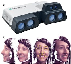
19. VCSELS for 3D sensing. Infrared dot fields are used for determining the shape and position of 3D objects, as in the Microsoft Kinect and, more recently, the Apple iPhone X. In fact, the iPhone X contains vertical-cavity surface-emitting laser (VCSEL) sources to project its dot pattern, which is used for its face ID system. Being compact and rugged, high-power VCSELs can also be used as light sources for time-of-flight 3D sensing systems. Engineers at Philips Photonics (Aachen, Germany) have created high-power wafer-level-integrated VCSEL arrays for scanning lidar in automotive applications—the VCSELs have extended cavities that enable their brightness to be increased by more than a factor of a thousand. (See "Vertical-cavity Surface-emitting Lasers: VCSEL arrays provide leading-edge illumination for 3D sensing," October 2017 issue; https://goo.gl/K6BPVs.)20. Spatial sensing software. A very different type of optical 3D sensing system developed at the Fraunhofer Institute for Applied Optics and Precision Engineering (IOF; Jena, Germany) consists of an IR illuminator, optics, and two cameras, with the addition of a specially tailored rotating filter placed between the light source and the lens—a technique well known from theatrical illumination devices as GOBO (goes before optics). The system delivers full spatial information from 1000 × 1000 pixels at a 36 Hz frame rate with a resolution of about 0.4 mm at a distance of 1.5 m. Applications include measurement of human faces to a resolution that an iPhone X could only dream of (see Fig. 5). (See "Spatial Sensing: Real-time 3D scanner delivers 36 high-resolution color images per second," February 2017 issue; https://goo.gl/Rqi3Ki.)
About the Author
John Wallace
Senior Technical Editor (1998-2022)
John Wallace was with Laser Focus World for nearly 25 years, retiring in late June 2022. He obtained a bachelor's degree in mechanical engineering and physics at Rutgers University and a master's in optical engineering at the University of Rochester. Before becoming an editor, John worked as an engineer at RCA, Exxon, Eastman Kodak, and GCA Corporation.


