Positioning: Silicon photonics manufacturing requires parallelism in alignment processes
In 2000, well before the telecom-driven photonics boom of 1997-2002 reached its sudden end, the term "photonomics" was coined to underscore the importance of process automation for the economic well-being of the industry. The economic examples presented in that work seem quaint today: 60 parts per hour per workstation. Compare that to today's silicon photonics manufacturing processes in which thousands of devices are minted per wafer. A pace of 60 parts per hour may have been blistering two decades ago, but now it would mean unsustainability in the current and future competitive landscape.
Since the end of that telecom boom, the industry has revived, driven by new applications such as streaming video, online music, smartphones, and cloud computing. The good news for the photonics industry and its new partner, semiconductor manufacturing, is that the potential seems limitless. The bad news is that these new devices must be efficiently manufactured in unprecedented volume and follow a steeply dropping cost curve over a historically short timeframe.
The key to succeeding in this new environment is that old lesson from 2000: automation, especially of the coupling-optimization steps that are fundamental to so many test and packaging operations from wafer to final assembly. But a different kind of automation is needed today compared to 2000 because today's devices are smaller and more complex, they behave in more difficult ways, and there are more of them that need to be tested and packaged.
Novel devices, new challenges
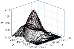
First, the clean, predictable Gaussians of previous single-mode couplings are no longer a given. Instead, silicon photonics couplings—from probing of devices when they are still on-wafer through multiple packaging and test steps of singulated chips and ancillary devices—can present complicated profiles, with multiple local maxima and saddle points surrounding a central, only quasi-Gaussian peak. Clearly, different optimization strategies are necessary compared to the comparatively simple alignment engines that emerged in the 1990s (see Fig. 1).
Besides the more complex couplings, there tend to be more of them per device. Silicon photonics devices can implement many channels, as well as inputs and outputs. The short waveguides of these devices mean the inputs and outputs often interact, making the overall global alignment a moving target.
For previous alignment automation technologies, this would dictate a time-consuming sequential loop of aligning this and then aligning that, returning and repeating to undo the impact of each successive alignment on its predecessors across the device, and then doing it all over again if drift should occur. Many of these alignments are sensitive to angle as well, requiring multiple optimizations across degrees of freedom as well as across inputs and outputs and channels.
In 2015, to meet these challenges, PI demonstrated the ability to perform alignments across multiple inputs, multiple outputs, and multiple degrees of freedom all at once, in parallel. This eliminated the successive loops of sequential alignments back and forth across the device and its channels. Instead, the global consensus alignment (including tracking if desired) is achieved in one fast step.
This alignment step alone can multiply the throughput from 60 devices per hour by two orders of magnitude, at least regarding the alignment steps. By eliminating the repetitive loops of sequential alignments, additional orders of magnitude of process throughput improvement can be readily achieved. This all means that alignment ceases to be the pacing item for overall device manufacturing.
Parallelism: The key to process economics
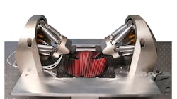
The importance of this to photonomics cannot be understated—this parallelism is an enabler for process economics at multiple nodes in the production chain, from verifying the functionality of devices while still on the wafer, to performing each assembly step, to validating the devices' health every step of the way, ensuring that bad or damaged products do not proceed through further costly packaging steps (see Fig. 2).
Besides the parallel optimization capability—which is founded on a novel revision of the classical digital gradient search—there is the need to achieve first-light in the first place and then to localize the main mode of each coupling to ensure against spurious lock-ons. Otherwise, the optimization risks locking onto one of the local optima rather than the global optimum.
This optimization can be efficiently achieved by performing an areal scan of the target area, and thereby mapping the coupling cross-section across its full extent. This was formerly performed in software and required significant time to accomplish, both because of communications latencies and settling dwells necessary at each end of each scan line in conventional raster and serpentine scans. Worse, most approaches have been based on pointwise move-and-acquire sequences, adding time-consuming settling and communications dwells at each data point in the scan.
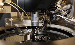
This software optimization process has all been rendered obsolete by two innovations: first, an entirely firmware-based command that leverages internal position-waveform and synchronous data acquisition, and then a single-frequency sinusoidal raster or spiral scan that proceeds smoothly and continuously while avoiding exciting structural resonances in mechanical elements like fibers and tweezers. The result is an orders-of-magnitude improvement in process throughput (see Fig. 3).
Aiding in the quest for more alignment speed are motion engines based on a parallel-kinematics design concept (see "Parallelism in the design approach of multi-axis motion systems" at the bottom of this page). By splitting the long travel motion system and the high-speed scanner (analogous to a multi-stage space rocket, where not all of the mass needs to be accelerated the whole distance), additional performance can be found.
Putting it all together is where the advantages of this fully modern architecture becomes evident. The single-frequency sinusoidal or spiral raster scan allows mapping of an entire coupling region with high resolution in about 250–300 ms, complete with the firmware-based fitting of a Gaussian to the observed coupling. This allows especially fast scans to be performed while still accurately localizing the main mode.
With the main mode localized at each coupling and each degree of freedom, the overall global consensus alignment across all inputs and outputs can be achieved in a few hundred milliseconds, with all optimizations performed in parallel. If desired (for example, to accommodate drift if it occurs, perhaps caused by heating from active elements, application of adhesive, or other disturbances), quick global realignment or even real-time tracking can then be performed.
Thus, to make silicon photonics devices profitably at scale, automation becomes an essential element in process-design engineering. Meeting this requirement, recent advances in fab-class process automation subsystems include innovations in one of the bedrock operations of photonics manufacturing—the alignment process, which is common to process steps from device characterization at the wafer level through final assembly and packaging.
REFERENCE
1. S. Jordan, "Alignment: A Challenge for Test & Measurement," https://goo.gl/pfiJgm.
Parallelism in the design approach of multi-axis motion systems
When faced with a multi-axis motion application, the traditional way is to stack multiple single-axis motion stages. As applications become more complex, so do the equivalent stacks of stages—and advantages such as simplicity can turn into disadvantages when it comes to performance.
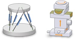
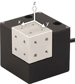
A parallel kinematics design provides a more effective approach to multi-axis motion and brings several advantages (see Fig. 1):
Dynamics/stiffness. With conventional multi-axis systems, the bottom stage in a stack carries the mass of the entire stack and so on up to the top stage, which carries only the application load. Dynamics suffers because of the overall moved mass and tuning becomes a laborious, axis-by-axis process, with different settings for each axis and consequently different responsiveness. Hexapods provide very high stiffness because all six struts work in parallel on one common lightweight motion platform. Consequently, the dynamics are higher and tuning settings are very close for all axes.
Rotation-centerpoint flexibility. Stacked stages place the center of their tip/tilt and rotation motions at the geometric centers of each rotation stage and goniometer bearing. Sometimes, they coincide at a desired point in space (for example, at the focal point of a lens) via custom adapter plates and fixtures, but this takes time and effort, and is inflexible should application requirements change. With hexapod multi-axis systems, the center of rotation can be changed by a single software command on the fly.
No moving cables. Managing cables deserves more attention than it often gets. Cables can be a conduit for vibration that can impact an entire application. As a stage moves, any cable being dragged along can contribute to parasitic motions and other errors. These issues scale with the number of axes in a user-stacked system. Parallel kinematics avoid moving cables and the other issues altogether.
Parasitic errors. Stacked axes interact in complicated ways. For example, runout in the x-axis can cause unwanted motion in the y- and z-axes; angular deviation of an axis similarly imparts motion in the travel-directions of the other axes, with magnitude proportional to the distance to the moving axis. And in stacks, that multiplicative lever arm can be large.
What works on a larger scale for long-travel positioners can also be implemented for motion with sub-nanometer resolution and sub-millimeter travel ranges. Piezo flexure positioners rely on motion based on the piezoelectric effect. An embedded piezo ceramic transducer changes its dimensions analogous to an applied voltage and a wire-EDM cut flexure arrangement amplifies the motion while providing frictionless guidance at the same time (see Fig. 2).
About the Author
Scott Jordan
Head of Photonics, PI (Physik Instrumente)
Scott Jordan is Head of Photonics at PI (Physik Instrumente; Auburn, MA).
Stefan Vorndran
Stefan Vorndran is VP of marketing at PI (Physik Instrumente; Auburn, MA).