Simulation and Modeling: Surface-plasmon modeling drives OLED design, cutting efficiency loss
SARAH FIELDS
Organic LEDs (OLEDs) are attracting strong interest because they can be used in lightweight, paper-thin, light-emitting panels in a variety of shapes and sizes. They can be used to create flexible or bendable lighting devices applied to a flat or curved surface area to create parts such as car taillights, architectural and specialty illumination, and other light sources.
But OLEDs aren't nearly as bright or as energy-efficient as their inorganic counterparts, LEDs, and so researchers at Konica Minolta (Tokyo, Japan) are developing designs to meet growing demand. The company supports the development of cutting-edge OLED devices for imaging and optics, often working in partnership with Japan's leading universities.
Researchers at the Konica Minolta Laboratory USA (San Mateo, CA), led by Leiming Wang, are using numerical simulation to analyze light-loss mechanisms in OLEDs to virtually test ways to improve designs. Despite all their advantages, OLEDs suffer from a number of limitations that the researchers are working to minimize. Most impactful is a complex plasmon coupling phenomenon that accounts for 40% of the light lost through interactions within the device.
How OLEDs work
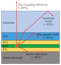
OLEDs are composed of organic semiconductors sandwiched between positive (anode) and negative (cathode) electrodes. Figure 1 shows the layout of an OLED device, with an anode made of transparent indium tin oxide (ITO), three organic layers—a hole-transport layer (HTL), an emitting layer (EML), and an electron-transport layer (ETL)—and a silver cathode. These are all fabricated on a glass substrate, which passes light when the device is turned on.
When current is applied, electrons are injected at the cathode and holes at the anode. Electrons and holes travel toward each other through the layers, combining in the emissive layer to release energy in the form of photons. This happens quickly while current is flowing, causing a stream of continuous light.
But some photons never make it to the outside world. Light losses in an OLED can occur through several mechanisms, such as differences in the refractive indices of each layer that can cause light to reflect within the layers rather than traveling outward (see Fig. 2).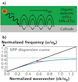
Wang's team primarily explored another mode of loss, the coupling of dipole emission with surface plasmons at the interface between the cathode and the organic material layer. Surface plasmons are waves of oscillating electrons on the surface of a conductor. In OLEDs, light emitted from radiating dipoles (molecular excitons) in the emissive layer can couple to the electron oscillations in the cathode, resulting in the presence of electromagnetic waves in the infrared or visible region of the spectrum called surface-plasmon polaritons (SPPs). These waves travel along the cathode surface as they decay, rather than permitting them to radiate through the glass (see Fig. 2a).
It is important to note that much of the recent interest in SPPs is because of their excellent confinement of electromagnetic energy beyond the diffraction limit. As a result, they are well represented in numerous areas of near-field optics, biosensing, and metamaterials.
Light loss through SPPs
However, in the optimization of an OLED, SPPs are a dominant loss factor. Because of the presence of the metal cathode in the close vicinity of the organic emitters, some light is absorbed by the electrons in the cathode, causing the electrons to oscillate and form the SPPs. These are eventually dissipated as heat, leading to significant energy loss. If the loss via SPPs can be reduced, the outcoupling efficiency of the OLED can be increased, which means better, more efficient lighting.
SPPs propagate along surfaces—but not just any surface. SPPs are found along an interface between two materials that have a different sign in their permittivity. Many common materials, such as air, water, plastic, and paper, have a positive permittivity. Metals like gold, silver, and aluminum have a negative permittivity, and so SPPs can exist at the interface between gold and air, for example.
Just because an SPP can exist at that interface, however, does not mean that it is trivial to generate and control them. Generating an SPP with a traditional light source such as a laser is slightly more complicated, as is the inverse process—converting an SPP to visible light as in an OLED.
To couple freely propagating light and SPPs, their dispersion curves need to intersect, which is analogous to matching the energy and moment of the two (see Fig. 2b). The diagonal black line represents the dispersion curve for light propagating freely in air, while the blue line is the dispersion curve for an SPP at an air/metal interface. The two lines approach each other asymptotically, but they do not intersect. There are several techniques to make these two curves meet, such as using a prism in either a Kretschmann or Otto configuration. Another technique is the use of a grating.
A grating has a regularly repeated pattern, like a sine wave or sawtooth pattern. The periodicity has its own wavevector, which can be added (or subtracted) to the wavevector of the SPP to allow dispersion curve matching, represented by the red arrow in the plot in Fig. 2.
Simulation using Maxwell's equations
Implementing the grating coupling numerically is straightforward using multiphysics simulation that solves for Maxwell's equations, which means that the coupling between free-space light and SPPs is inherently accounted for without any additional modifications.
Using numerical simulation in software by COMSOL (Burlington, MA), Wang modeled light emission from the EML and the SPPs present in the system to analyze ways to prevent light loss. One promising concept included a nanograting cathode structure (see Fig. 3a) that disrupts the formation of the SPP mode, reducing the energy coupling between the dipole emission and the plasmons.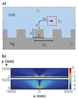
Wang's simulation results revealed the electromagnetic field distribution and the proportion of light that escaped from the OLED for different cathode shapes (see Fig. 3b). From the model results, his team was able to confirm that this phenomenon accounts for significant portions of the light lost.
His team modeled the OLED with flat and nanograting cathodes, changing geometric parameters to determine the optimal configuration (see Fig. 4). They also performed a simulation to study the influence of different dipole orientations, studying the effect of the dipole position and wavelength on the level of light loss because of SPPs.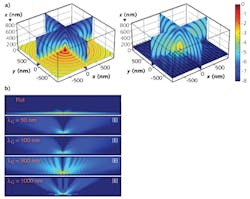
They used a power-flow analysis to calculate the portion of light emitted from the EML that actually escaped the glass. Through their simulations, Wang's team determined that they could reduce the plasmon losses by 50% using the optimized nanostructure surface in the cathode.
Versatile modeling brings brighter lighting
Through his simulation work, Wang was able to offer a promising new OLED design with significantly increased efficiency. The use of Multiphysics modeling software allowed the researchers to not only understand the breakdown of loss mechanisms, but to easily test the influence of different design constraints and adjust the OLEDs accordingly, allowing plasmon losses to be cut in half.
Sarah Fields is a technical marketing engineer at COMSOL, Burlington, MA; e-mail: [email protected]; www.comsol.com.