Integrated Photonics: 2D dichalcogenides promise efficient electronic-photonic integrated circuits

A single material platform is desirable for monolithic integration of photonic and electronic circuits. In 1958, Jack Kilby of Texas Instruments realized the importance of making all electrical components on the same semiconductor and demonstrated the first integrated circuit (IC). The problem with conventional semiconductors is that even if they can emit light, they cannot absorb the light at the same wavelength because of weak absorption at their bandgaps. In other words, optical communications between the detector and transmitter cannot be implemented on the same material without expensive wavelength conversion or hybrid materials schemes.
However, two-dimensional (2D) transition metal dichalcogenides (TMDs) are emerging as a new class of semiconductor nanomaterials promising for both electronic and photonic device applications. The emission-absorption resonance in TMDs, or the ability of the materials to both emit and absorb light at the same wavelength, is made possible by their large exciton binding energies. These 2D TMDs have exceptional optical and electrical properties, and they have been used to make electronic and optoelectronic devices such as field-effect transistors, photodetectors, light-emitting diodes, and lasers.
Using 2D TMDs, scientists from the University of Electronic Science and Technology of China (UESTC; Chengdu, China), the University of Houston, Rice University (both in Houston, TX), and Baylor University (Waco, TX) have demonstrated resonant optical generation and detection of surface-plasmon polaritons (SPPs) by tungsten disulfide (WS2), a TMD proving that 2D TMD materials are ideal for electronic-photonic ICs.1
On the same wavelength
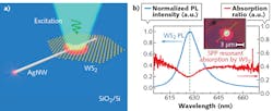
The scientists synthesized monolayer WS2 on substrates using chemical vapor deposition. A silver nanowire with a diameter of 120 nm was then placed onto the monolayer WS2 and used as a plasmonic waveguide. Under 532 nm laser excitation through a microscope objective, the photoluminescence (PL) from WS2 was coupled to the SPP in the silver nanowire. The scientists found that the spectrum of SPP re-absorption by WS2 perfectly overlapped with the WS2 PL spectrum. It is the first time that optical emission and absorption resonance was observed for SPPs in the same semiconductor material.
In further experimentation, it was determined that the effect of WS2 is strong regardless of the nanowire's diameter. For the 120 nm nanowire, a propagation length of 2.4 μm is obtained, which is in good agreement with the experimental value. In addition, the SPP wavelength can be selected by choosing different TMDs or tuned by straining or doping. Although the generation and detection of SPPs was demonstrated optically, the device can be readily modified to perform local generation and detection of SPPs by electrical means. That is, nanoscale optical communications between transistors on the same TMDs is possible.
The plasmonic waveguide can also be lithographically defined. Since the planar structure of 2D TMDs is compatible with the current lithographic fabrication process, such devices can be easily integrated into an on-chip electronic-photonic integrated circuit (EPIC). The scientists are currently working on the demonstration of a complete EPIC based on this discovery.
"The observation of emission-absorption resonance is surprising," says Jiming Bao, associate professor in the department of Electrical and Computer Engineering at the University of Houston. "Initially we only wanted to study the coupling of light from WS2 to a silver nanowire. We expected that the surface plasmon from the silver nanowire end had the same wavelength as WS2 photoluminescence, but a significant redshift of the surface plasmon prompted us to perform systematic spectral analysis and then we found the resonance. We are also exploring more applications from other TDMs such as MoS2, WSe2, and MoSe2. I believe more and more research results on TDMs will appear in the near future from different research groups."
REFERENCE
1. Z. Zhu et al., ACS Photon., 3, 5, 869–874 (2016).
About the Author

Gail Overton
Senior Editor (2004-2020)
Gail has more than 30 years of engineering, marketing, product management, and editorial experience in the photonics and optical communications industry. Before joining the staff at Laser Focus World in 2004, she held many product management and product marketing roles in the fiber-optics industry, most notably at Hughes (El Segundo, CA), GTE Labs (Waltham, MA), Corning (Corning, NY), Photon Kinetics (Beaverton, OR), and Newport Corporation (Irvine, CA). During her marketing career, Gail published articles in WDM Solutions and Sensors magazine and traveled internationally to conduct product and sales training. Gail received her BS degree in physics, with an emphasis in optics, from San Diego State University in San Diego, CA in May 1986.