Materials for Light Sources: 2D materials challenge QDs and phosphors for color conversion
A U.S. patent granted to VerLASE (Winooski, VT) describes new wavelength-conversion materials based on two-dimensional (2D) semiconductor structures that overcome most technical issues associated with traditional phosphors and even overcome emerging hurdles to adoption of quantum dots (QDs).1
Compared to traditional phosphors, these 2D converters have a narrower spectral profile and better color saturation. And compared to both QDs and phosphors, the new materials have better thermal properties and are self-passivated, with minimal dangling chemical bonds. The latter can cause blinking and nonreversible photobleaching when using QDs.
‘Flat’ 2D structures
Just like QDs that downconvert to visible colors based on their size and material properties, the 2D converters are also quantum-confined structures, but act as quantum wells (QWs). They present in a “flat” orientation as nanoplatelets that can be fabricated by exfoliating 2D crystals grown at high speed as small crystallites in a furnace for very low cost. These crystals, which grow as layered materials, can include gallium selenide (GaSe), gallium sulfide (GaS), tungsten disulfide (WS2), and others, where the layers are weakly bound to each other and create photoluminescent quantum wells when separated into thin-enough nanoplatelet structures. They are physically anisotropic with micron-scale sizes in the plane, but nanoscale in thickness, which also allows them to be laid flat using deposition techniques.
When excited by blue LEDs, for example, these nanoplatelets re-emit light in difficult-to-produce colors including reds, greens, and yellows depending on the material used and thinness, akin to the core of QDs without their shell structure. They are just QWs, which are 2D films, but operating like QDs, which are zero-dimensional quantum-confined structures, with diameter rather than thinness used to control discrete quantized energies in the density of states (DOS).
These 2D semiconductor materials can be used as they are, immediately upon fabrication, sandwiched by air or layers of other exfoliated 2D materials, or combined with layers of other higher-bandgap semiconductor materials, modifying the QW region and simultaneously altering the resultant downconversion properties.
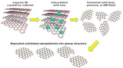
Exfoliation refers to delaminating the crystallites into just a few layers or even a monolayer and takes advantage of techniques developed for making graphene, such as mechanical grinding and ultrasonic agitation, use of supercritical fluids, or chemical intercalation of a species between the layers that breaks apart the layers with heat, microwaves, or other stimuli. Exfoliation can be controlled for uniform thinness of 2D nanoplatelets that can then be laid down through roll-to-roll techniques or embedded into a polymer matrix (see figure).
For example, the process can be used to create flat sheets of gallium selenide QW nanoplatelets that emit in the 610–620 nm range with a 30–40 nm bandwidth, and paired with standard solid-state lighting materials to produce a warm white light. These 2D downconversion sheets can be fabricated into numerous forms for use in displays, projection systems, and luminaires, and can also be extended with other material sets into infrared and ultraviolet regions.
“We have shown RGB [red, green, and blue] colors by just thinning QWs exfoliated from the same bulk gallium selenide crystals,” says George Powch, VerLASE CEO. “We are also working on electroluminescent versions—an objective QDs have yet to achieve. Such devices would use all inorganic materials and be manufacturable at low cost by levering existing semiconductor fabs.” VerLASE is currently seeking partners to help bring the technology to market.
REFERENCE
1. US Patent No. 9,035,344 (Jun. 15, 2015).
About the Author

Gail Overton
Senior Editor (2004-2020)
Gail has more than 30 years of engineering, marketing, product management, and editorial experience in the photonics and optical communications industry. Before joining the staff at Laser Focus World in 2004, she held many product management and product marketing roles in the fiber-optics industry, most notably at Hughes (El Segundo, CA), GTE Labs (Waltham, MA), Corning (Corning, NY), Photon Kinetics (Beaverton, OR), and Newport Corporation (Irvine, CA). During her marketing career, Gail published articles in WDM Solutions and Sensors magazine and traveled internationally to conduct product and sales training. Gail received her BS degree in physics, with an emphasis in optics, from San Diego State University in San Diego, CA in May 1986.
