PHOTONIC FRONTIERS: NANOLASER PROGRESS: Surface plasmons and nanolasers: A big push for very small lasers
Hybrid semiconductor-metal lasers are making big progress on the nano frontier, scaling to smaller sizes and continuous-wave operation. But theorists warn that reducing size too much will increase losses, limiting how far lasers can shrink.
Microlasers aren't small enough when it comes to integrating lasers with electronics on solid-state circuits. State-of-the-art electronic chips have features just tens of nanometers across, but today's diode lasers have micrometer-scale structures. How can lasers be squeezed down to the size of electronic circuit components?
It's a tough problem, because conventional optical resonators must be on wavelength scales, and optical wavelengths are hundreds of nanometers and up, more than an order of magnitude larger than chip features. However, developers have found that they can use surface plasmons—compact clusters of electrons oscillating at optical frequencies—to squeeze lasers to the nanoscale, with volumes below a cubic wavelength. The first nanolasers could only emit pulses, but continuous-wave (CW) versions have been reported in the past year. The big questions now are how small can they be made and how practical can they become?
Surface plasmon basics
Light-emitting dielectric cavities must be large enough for half a wavelength to fit in each direction, but cavities can be made smaller by incorporating metals into a composite structure. Electrons at the interface between a metal and a dielectric or a semiconductor can oscillate coherently at optical frequencies, an effect called a surface plasmon, which can be excited electrically or by interaction with a photon. A surface plasmon can couple with a photon to produce a surface plasmon polariton, a hybrid oscillation that propagates along a metal-dielectric surface.
Surface plasmons and polaritons oscillate over areas smaller than the corresponding optical wavelength. That behavior is like the oscillation of electrons in radio-frequency antennas, which can transmit or receive radio wavelengths longer than the antenna. Recently nanolasers have reached volumes smaller than the cube of the wavelength in vacuum, although like radio antennas, nanolasers often are long and thin, so at least one dimension remains longer than the wavelength. Typical of a young field, the terminology can be muddled; although all nanolasers rely on surface plasmon effects, only a fraction of developers call their devices "spasers," for Surface Plasmon Amplification by the Stimulated Emission of Radiation -- a term coined nearly a decade ago.1
Martin Hill of the Technical University of Eindhoven (Eindhoven, the Netherlands) demonstrated the first metal-semiconductor nanolaser in 2007.2 That launched a wave of demonstrations of pulsed nanolasers that I described in 2011.3 The past year has seen further demonstrations of several designs, including the first CW nanolasers. By convention, device size is compared to the wavelength in vacuum λ rather than the actual wavelength λ/n in a material of refractive index n.
Goldfingers
Hill's initial plasmon nanolaser was a pillar of compound semiconductor coated with a layer of gold, earning the design the nickname "goldfinger." The fundamental concept is to generate light by coupling light amplification in the semiconductor gain material with surface plasmons at the metal-semiconductor interface.
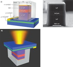
In January, Cun-Zheng Ning of Arizona State University (Tempe, AZ) and colleagues including Hill reported using that approach to make the first electrically excited subwavelength laser emitting CW at room temperature.4 The central rectangular pillar was a stack of three layers, n-doped indium phosphide (InP), undoped indium gallium arsenide (InGaAs), and p-doped InP, on a substrate as shown in Fig. 1, with the refractive-index difference confining light emission largely in the higher-index InGaAs. Coating the pillar with a 20 nm layer of silicon nitride on all four sides produced a structure 0.34 μm wide, 3 μm long, and 1.53 μm high. Then they coated the pillar, but not the substrate, with silver to form a metal-insulator-semiconductor-insulator-metal waveguide.
Light is generated in the red InGaAs active layer and oscillates along the length of the cavity, but can penetrate only 10 to 20 nm into the silver covering the pillar. Light instead is coupled through the unmetallized substrate. Laser emission at room temperature was CW in a 4 nm band centered on 1554 nm, corresponding to a Q factor of 400, solid evidence of lasing. At that wavelength, the semiconductor structure corresponded to 0.42 cubic wavelength in vacuum. Ning's group reported that heating limited device performance, and said they planned to improve device design and thermal packaging.
At CLEO in May 2012, they reported reducing losses by increasing the silicon nitride (SiN) cladding to 30 nm to better isolate the core from the lossy metal cladding, and by depositing up to 2 μm of silver to increase grain size. That improved cavity Q and reduced linewidth to 0.54 nm in a 1.15 × 1.39 × 1.7 μm (0.67 λ3) cavity.4 The electrical excitation is an important advantage for potential electronic applications.
Coaxial nanolasers
An optically pumped coaxial nanolaser structure also has emitted CW at room temperature, and at 4.5 K has demonstrated thresholdless emission near 1400 nm. At its center is a metal rod, like the central conductor in coaxial cable. As shown in Fig. 2, a ring of semiconductor surrounds the rod and is in turn coated with metal like the outer shield on coaxial cable. On one end is a metal cap, separated from the semiconductor by a silica layer. The other end of the structure is open to the air but recessed from the end of the coaxial coating.
As in the goldfinger structure, the semiconductor structure is layered, with light generated in six InGaAsP quantum wells with gain from about 1.26 to 1.59 μm. The impedance mismatch between the semiconductor and free space creates a high-Q resonator, which supports only a single resonant mode and couples weakly to modes in free space. Shaya Fainman's group at the University of California at San Diego (La Jolla, CA) tested two designs, one with a 100 nm core surrounded by a 100 nm ring, the other with a 175 nm core and 75 nm ring. The thicker-ring structure lased at room temperature, but Fainman says that reaching thresholdless operation required scaling down the ring for singlemode operation. That reduced gain, so it was cooled to 4.5 K, where they observed narrow-line emission for pump powers from the noise floor of 0.72 nW to more than 100 μW, they reported in Nature in February.6 That's potentially important because it promises very efficient conversion of current into photons for optical communications on chips.
Single-crystal silver for high efficiency
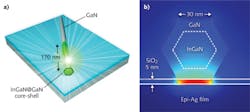
In July 2012, an international team led by Chih-Kang "Ken" Shih of the University of Texas at Austin (Austin, TX) and Shangjr Gwo of the National Tsing-Hua University (Hsinchu, Taiwan) reported the first CW operation of a third type of plasmonic laser, originally demonstrated in pulsed mode by Xiang Zhang's group at the University of California at Berkeley (Berkeley, CA).7 The idea is to optically excite laser emission in a semiconductor nanorod lying on a metal slab covered with a thin insulating layer.
The team used a hexagonal GaN rod 480 nm long that contained a 170-nm-long core of InGaN and faces 30 nm wide. It rested on a 5 μm silica film deposited on a 28 nm layer of single-crystal silver with an atomically smooth surface, as shown in Fig. 3.8 The single-crystal silver reduces laser threshold by three orders of magnitude compared to the polycrystalline metal used in earlier experiments, says Gennady Shvets, a Texas physicist who coauthored a report in Science.8 Surface roughness and grain boundaries in polycrystalline silver scatter surface plasmon polaritons so they release energy along the length of the structure; with single-crystal silver, they release light only at the ends of the structure, which Shvets and Shih call a "spaser." Pumping with a 405 nm blue diode generated laser emission from the InGaN core peaking at 510 nm. Emission was highest at 8 K and disappeared above 80 K from the laser, which they call the world's smallest semiconductor laser.
Outlook
The small emitting area of nanaolasers is good because it allows low threshold and fast modulation but challenging because the emission spreads rapidly. Zhang hopes to improve directionality, to make nanolasers more attractive for applications such as on-chip communications.
Nanolaser development reminds Fainman of VCSEL development 25 years ago. "Nobody knew what it was good for, and performance was poor compared to edge emitters, but today if you buy a new computer, it has a VCSEL sitting there with a fiber output," he says. Although nanolasers are immature today, they may be ready in a couple of decades.
Shvets envisions potential applications in exciting materials that cannot withstand high flux, such as in biosensing. He is particularly interested in advanced nonlinear spectroscopy of molecules.
Nanolasers can be small in two dimensions, but they must be long enough in a third dimension to hold at least a half wavelength in the material, says Jacob Khurgin of Johns Hopkins University (Baltimore, MD). Metal can confine light, but squeezing the cavity smaller pushes more light into the metal, where it suffers very high losses, raising the threshold. For electrical excitation, he calculates threshold current would be ~10 μA, corresponding to an impractical current density of ~100 kA/cm2. A better nanoscale light source, he suggests in Nanophotonic, would be a subminiature version of the LED, a "Surface Plasmon Emitting Diode (SPED)."9 Time will tell if he's right.
REFERENCES
1. D.J. Berman, and M.I. Stockman, "Surface plasmon amplification by stimulated emission of radiation: Quantum generation of coherent surface plasmons in nanosystems," Phys. Rev. Lett., 90, 027402 (2003).
2. M.T. Hill et al., "Lasing in metallic-coated nanocavities," Nature Photon., 1, 589 (2007).
3. J. Hecht, "Photonic Frontiers: Novel Lasers--The incredible shrinking laser makes a big impact," Laser Focus World, 47, 10, 41-45 (Oct. 2011).
4. K. Ding et al., "Room-temperature continuous wave lasing in deep-subwavelength metallic cavities under electrical injection," Phys. Rev. B, 85, 041301(R) (2012); doi:10.1103/PhysRevB.85.041301.
5. K. Ding et al., "Record Performance of a CW Metallic Subwavelength-Cavity Laser at Room Temperature," CLEO 2012 Tech. Dig., paper CTh4M.3.
6. M. Khajavikhan et al., "Thresholdless nanoscale coaxial lasers," Nature, 482, 204 (Feb. 9, 2012); doi:1RI40.
7. R.F. Oulton et al., "Plasmon lasers at deep subwavelength scale," Nature, 461, 629-632 (Oct. 1, 2009); doi:10.1038/nature08364.
8. Y.-J. Lu et al., "Plasmonic Nanolaser Using Epitaxially Grown Silver Film," Science V, 337, 450 (July 27, 2012).
9. J.B. Khurgin and G. Sun, "How small can 'Nano' be in a 'Nanolaser'?" Nanophoton., 1, 3-8 (2012); doi:10.1515/nanoph-2012-0017.
About the Author
Jeff Hecht
Contributing Editor
Jeff Hecht is a regular contributing editor to Laser Focus World and has been covering the laser industry for 35 years. A prolific book author, Jeff's published works include “Understanding Fiber Optics,” “Understanding Lasers,” “The Laser Guidebook,” and “Beam Weapons: The Next Arms Race.” He also has written books on the histories of lasers and fiber optics, including “City of Light: The Story of Fiber Optics,” and “Beam: The Race to Make the Laser.” Find out more at jeffhecht.com.


