FLEXIBLE DISPLAYS: Sheetlike microplasma arrays have many applications
J. GARY EDEN and SUNG-JIN PARK
Plasma, also known as the fourth state of matter, is a partially ionized gas or vapor. Commercial applications of plasmas include water purification, manufacturing of integrated circuits, and curing polymers, but of all the industrial and residential uses of plasma, displays and lighting are pre-eminent. The rise of flat-panel plasma TVs in the past decade has been nothing short of meteoric. However, despite the recent emphasis by manufacturers on decreasing the power consumption and thickness of plasma and liquid-crystal-display (LCD) TVs, the most pressing long-term drivers of display development continue to be dramatic reductions in weight and manufacturing cost, as well as the introduction of flexibility. The availability of an economical sheetlike flexible display that could be hung on a wall, or wrapped around curved surfaces, would allow video displays to be placed virtually anywhere for a variety of applications.
In the realm of lighting, plasma lamps have a dominant position by generating several gigawatts of visible light on a continuous basis worldwide, or approximately 80% of all the light produced by general illumination. Although existing plasma lamps boast favorable efficiencies, virtually all contain mercury and most require ballast and have a fragile glass envelope. The availability of a thin, lightweight, inexpensive, and nontoxic source of white light would transform the landscape of residential and commercial lighting.
Microcavity arrays
The emerging field of microplasma technology holds considerable promise for the next generation of displays and lighting. By shrinking a conventional plasma lamp by three orders of magnitude, microscopic plasmas having the form of cylinders, ellipsoids, or other shapes can be generated by the thousands or millions in microcavities fabricated in the surface of glass, aluminum (Al) foil, or even plastic. Having sizes on the order of the diameter of a human hair, these microcavities are built by processes largely developed by the very-large-scale-integration (VLSI) and MEMs communities.
By successfully confining plasmas in arrays of microcavities, researchers and engineers at the University of Illinois have realized light-emitting sheets that are thin and inexpensive and, in several instances, flexible as well. At the heart of a microplasma device is the microcavity itself, whose shape, in addition to the surrounding materials determines the spatial profile of the electric field within the cavity. Most of the microplasma devices being pursued today are cylindrical with diameters of 50 to 200 µm, but other cross-sectional shapes such as diamond, rectangular, and pyramidal have also been created and used successfully, and the smallest plasmas realized to date were confined to cavities 5 µm in width.
A wide array of substrate materials, including silicon, glass, high-k ceramics, polymers, and Al have been explored. After sealing the device (or a large array of devices) with a window material, a gas or mixture of gases is introduced to the cavity. With proper design of the electrodes, the dielectric separating them, and the cavity, a stable and bright glow discharge is produced in the microcavity when a voltage (AC, DC, or pulsed) is applied to the electrodes.
Near-atmospheric pressure
Although in some ways similar to plasmas in standard fluorescent lamps, microplasmas have several startling properties. Because of their small cavity dimensions, microplasma devices operate well at pressures of roughly one atmosphere, as opposed to the several thousandths of an atmosphere that is characteristic of fluorescent lamps. This property is valuable for several reasons, one of which is that little or no pressure differential exists across the window and substrate of a microplasma lamp, thereby allowing the overall package to be quite thin and flexible. A less obvious advantage is the ability to produce efficiently, in large numbers and in situ, transient light-emitting molecules not normally found in nature (such as excited diatomic xenon or argon deuteride).
Another surprising characteristic of microplasmas is the steady-state power loading, or power density (electrical power deposited in the plasma per unit volume), which often reaches tens of kilowatts per cubic centimeter; values as high as 1 MW/cm3 have been realized. Such excitation levels are extraordinary and, in fact, unprecedented for continuous operation of macroscopic plasmas. For comparison, the power loading of fluorescent lamp plasmas is typically tens to hundreds of milliwatts per cubic centimeter.
To meet the need for inexpensive, large-area display and lamp technology, arrays of microplasma devices built into Al foil were first tested successfully four years ago at the University of Illinois; the development curve has been steep ever since. Aside from the low cost of Al foil itself, a strong attraction of this technology is the automatic formation of array electrodes and interconnects by a wet chemical process.
Beginning with a single sheet of Al foil having a thickness of nominally 120 µm, holes or cavities 30 to 200 µm in diameter are produced in the foil in the desired pattern by etching. In a subsequent electrochemical process, virtually all of the Al in the original foil is converted into translucent, nanoporous Al oxide (Al2O3). This carefully controlled wet process forms electrodes around the microcavities and the electrical interconnects between microcavities while simultaneously burying the microplasma devices in a thin layer of Al2O3.
Converting aluminum to alumina
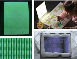
If the cavity-to-cavity spacing (pitch) and chemical-processing parameters are chosen properly, the electrodes for all of the microcavities in a line (or a two-dimensional pattern, if desired) are interconnected automatically. A modification of this process provides the ability to precisely control the cross-sectional geometry of a cavity, thereby opening the door to shaping the electric field throughout the microplasma while also optimizing the extraction of light from the cavity. For example, an array of 20,000 micro-emitters, each having a parabolic cross-section and an emitting aperture of 160 µm, has been fabricated (see Fig. 1). This array has a radiating area of about 25 cm2 and, although originally a 120 µm thick sheet of ordinary Al foil, has been almost entirely converted into transparent alumina. The green luminescence from the array is the result of injecting a commercial phosphor into each microcavity and illuminating the array with weak ultraviolet light.
Such arrays are the building blocks for displays and lamps. Microplasma lamps as large as 900 cm2 in active (radiating) area have been built and tested to date but development at Eden Park Illumination is focusing on 6 × 6 in.2 (230 cm2) and 8 × 8 in.2 (400 cm2) white lamps. Having a thickness of only a few millimeters, these flat lamps are powered by plasmas produced within cavities in a phosphor and alumina-overcoated Al mesh. A carefully balanced mixture of red, green, and blue phosphors converts ultraviolet emission generated by the rare-gas plasmas into white light. Although optimizing the cavity design and other aspects of the lamp's construction is in progress, the luminous efficacy (optical efficiency, expressed in units of lumens/watt) of these first-generation lamps easily exceeds that of incandescent lamps, and laboratory prototypes are yielding efficacies beyond 30 lumens/W.
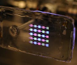
Arrays of microplasmas are also promising for environmental applications such as the purification of air or ozone production. A small array has been made that operates continuously in ordinary room air, for example, a feat which is extraordinarily challenging with conventional (macroscopic) plasma technology. By producing intense but uniform glow discharges in air, biological contaminants can be destroyed and pollutants or greenhouse gases converted into other, more useful forms.It is flexibility, however, that may well be the most appealing aspect of microplasma technology. Displays made by sealing microplasma arrays within thin plastic sheets are both flexible and transparent, such as shown in the low-resolution prototype in Fig. 2. Cavities and gas-connecting channels are stamped into the plastic substrate by a process known as replica molding; addressability of all the pixels in such arrays has been achieved. With this development, lightweight wall-sized plasma TVs can be envisioned that could ultimately lead to widespread adoption of virtual-reality environments.
J. Gary Eden and Sung-Jin Park are professors of electrical and computer engineering at the University of Illinois, 1406 W. Green, Urbana, IL 61801, and cofounders of Eden Park Illumination, 903 N. Country Fair Dr., Champaign, IL 61821; e-mail: [email protected]; www.edenpark.com.

