UV DETECTORS: Nitride-based UV detectors improve photodetection
MIRA MISRA, ANIRBAN BHATTACHARYYA, AND THEODORE D. MOUSTAKAS
Compared to ultraviolet detectors based on traditional semiconductors like silicon and gallium arsenide, nitride-based UV detectors have improved insensitivity to visible and infrared radiation, high responsivity, low noise, superior radiation hardness, and better operation at high temperatures.
Ultraviolet (UV) detectors are used in scientific research, industrial, and military applications, and must be either “visible blind” or “solar blind” to detect a weak UV signal in the presence of strong ambient light. Nitride-based UV detectors, unlike those based on traditional semiconductors such as silicon and gallium arsenide, are making strides in detecting UV radiation—from 400 nm to x-rays, as well as alpha particles—with improved sensitivity, high spectral selectivity and responsivity, and low noise.
With these advances, nitride-based UV detectors are finding use in areas such as the detection of UV flames for combustion control, surveillance of rockets and intercontinental ballistic missiles, secure space-to-space communication, detection of UV scintillation for medical imaging, monitoring of pollutants like nitrous oxide and sulfur dioxide in the ionosphere, in space-based instrumentation for UV astronomy, and in UV photolithography for semiconductor processing.
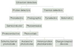
In general, UV detectors are classified as either photon or thermal detectors, depending on the mechanism of detection (see Fig. 1). Here, we limit our focus to photon detectors, which can be classified as either photoelectric or photographic. Photographic detectors are used for imaging high-energy radiation because they allow the recording of a large amount of data in a single exposure. However, they have a number of disadvantages: their sensitivity is lower than that of photoelectric detectors, their spectral response is wide, and their responsivity is not a linear function of the incident photon flux at a given wavelength. Photoelectric detectors—based on either photoemissive or semiconductor materials—are able to overcome these limitations and offer better performance.
Photoemissive UV detectors
The most commonly used photoemissive UV detectors are photomultiplier tubes (PMTs) with UV-transmitting quartz windows. This type of PMT is relatively expensive and its quantum efficiency in the spectral region below 300 nm is typically about 30% to 40%. Furthermore, PMTs are bulky, have high voltage and high power requirements, and are sensitive to magnetic fields.
Photoemissive array detectors such as microchannel plates (MCPs) combine high sensitivity and radiometric stability with high-resolution-imaging capability. Because these detectors make use of the external photoelectric effect, the wavelength range of sensitivity is determined by the work function of the photoemissive material.
Semiconductor UV detectors
The extremely strong absorption and radiation-induced aging effects in most semiconductor materials has historically hampered the development of high-quantum-efficiency semiconductor UV detectors. Semiconductor UV detectors can be made to operate either in the photoconductive or the photovoltaic mode. These photovoltaic detectors can have the form of a Schottky barrier, p-i-n diode, avalanche photodiode, heterojunction phototransistor, or be charge-coupled devices (CCDs).1
Silicon UV photodetectors are the most popular semiconductor UV detectors because of the maturity of the silicon (Si) material. To overcome the problem of absorption of UV photons in the top dead-layer of the diode, Si diodes for UV detection are fabricated with the junction very close to the surface, and are passivated by a very thin oxide layer. These devices exhibit external quantum efficiency in the 50% to 70% range, and are sensitive to 120 nm. However, they are inherently sensitive in the visible and infrared range of the spectrum and can be made visible or solar blind only by the addition of external optics.
Wide-bandgap semiconductor UV photodetectors include the chief contenders made from silicon carbide (SiC), diamond, and aluminum gallium nitride (AlGaN) alloys. Our group at Boston University focuses on UV detectors based on AlGaN alloys, with particular emphasis on recent studies of the materials characteristics that make this family of semiconductors unique for UV detectors.
AlGaN-based UV detectors
The gallium nitride, aluminum nitride (GaN-AlN) material system is well suited for UV photodetectors because its direct bandgap can be tuned from 360 to 200 nm by changing the alloy composition, enabling true visible-blind or solar-blind detectors (see Fig. 2). In addition, nitride semiconductors exhibit good electronic transport properties; they are physically robust, chemically inert, have high corrosion resistance, and are nontoxic. These properties also make them attractive for use in hostile environments and at high temperatures. These AlGaN alloys have been used to fabricate either photoconductive or photovoltaic UV detectors.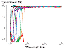
Photoconductive detectors are fabricated from AlGaN alloys in thin-film form with interdigitated metal contacts placed on the surface of the material to maximize light transmission while minimizing transit time. These photoconductive detectors, as opposed to photovoltaic ones, exhibit the important advantage of internal gain, which reduces the requirement for low-noise preamplifiers. The gain is due to the fact that the minority carriers are trapped while the majority carriers go around the circuit many times before recombination. Of course the fundamental principle in all detectors is that the gain times the bandwidth should be constant. Thus, if the detector is designed to have high photoconductive gain, its response time is long.
The photoconductive gain is given by the expression:
G = µτV/d2 = τ/tr
Here, µ is the electron mobility, t is the carrier lifetime, V is the applied bias voltage, d is the inter-electrode spacing and tr is the carrier transit time.
Thus, the gain in photoconductive detectors occurs because the recombination lifetime is much longer than the transit time. As a result, while the gain depends on the dimensions of the device and the applied voltage, the (µt) product—determined from the gain measurements—is the real figure of merit of the material.
The values of the photoconductive gain and responsivity of AlGaN UV detectors, reported by various groups, were found to vary widely.2-4 To find the origin of this variation, we fabricated a number of UV photoconductive detectors from GaN of various resistivities and AlGaN of various compositions and determined the (µt) product from the gain measurements (see Fig. 3).5-7 It is evident from these data that the (µt) product in these photodetectors varies by many orders of magnitude and is a strong function of resistivity of the semiconductor. Thus, by using GaN or AlGaN, UV detectors can be fabricated with either high gain/low speed, or vice versa.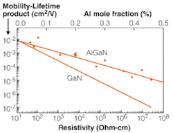
Notably, AlGaN photodetectors have higher (µt) products than GaN ones, even though they are expected to have lower mobility than GaN because of alloy scattering and shorter lifetime than GaN because of their more defective nature. To account for this anomaly our group investigated the structure of the AlGaN alloys and found that these materials consist of domains that are atomically ordered and others that have random alloy structure (partial ordering).8 Based on this finding we proposed that the band structure of the ordered and random domains form a type-II heterostructure. Thus, the electron-hole pairs created by the illumination are separated in the ordered and random domains, which leads to the observed enhancement of the lifetime. Recent theoretical calculations confirm the hypothesis of the type-II heterostructure in partially ordered AlGaN.9
Other important characteristics of these photoconductive detectors are their spectral response and dynamic range. Khan and our group reported that the spectral response of GaN photoconductive detectors shows a sharp increase by several orders of magnitude at the wavelength corresponding to the energy gap of the material and at shorter wavelengths the photoresponse remains constant. This needs to be contrasted with conventional semiconductors, like Si and GaAs, where the photoresponse drops drastically at short wavelengths, a result attributed to surface recombination. The constant photoresponse at short wavelengths in AlGaN photoconductive detectors is evidence that surface recombination is less important in these materials, consistent with their strong ionic character.10 The constant photoresponse at short wavelengths accounts for our observation that these detectors can also be used to detect x-rays and alpha particles. The dynamic range of GaN photoconductive detectors was also measured and the response was found to be linear over five orders of magnitude of incident power.
Finally, we investigated the noise characteristics of a number of GaN UV photoconductive detectors.11 The noise spectrum for low-resistivity material is dominated by 1/f and thermal noise, while for high resistivity material it is dominated by generation-recombination (G-R) noise. The noise equivalent power for the semi-insulating detectors was measured to be 3 × 10-14 W/Hz1/2 at 10 KHz.
Photovoltaic UV detectors based on AlGaN have been fabricated in the form of Schottky barriers, p-i-n diodes, phototransistors, and avalanche photodiodes. For example, visible-blind GaN p-i-n photodiode arrays with peak responsivity of 0.198 A/W at 360 nm corresponding to 85% internal quantum efficiency have been reported, with visible rejection of four to five orders of magnitude.12 By alloying GaN with AlN, these devices can be completely solar blind. To design such devices, one must take into account the fact that there is a reduction in the solar radiation between 240 and 280 nm due to ozone absorption. Therefore, for an AlGaN p-i-n diode, the composition of the n-layer should be chosen to absorb any UV light at wavelengths shorter than 240 nm. Also, the i-layer should be chosen to have an absorption edge at 280 nm.13
REFERENCES
- M. Razeghi and A. Rogalski, J. Appl. Phys. 79, 7433 (1996).
- M.A. Khan et al., Appl. Phys. Lett. 60, 2917 (1992).
- M. Misra et al., Proc. SPIE 2519 (1995).
- J.C. Carrano et al., J. .Appl. Phys. 83, 6148 (1998)
- M. Misra et al., Appl. Phys. Lett. 74, 2203 (1999).
- T.D. Moustakas and M. Misra, Proc. SPIE 6766, 67660C (2007).
- G. Mazzeo et al., Solid State Electron. 52, 795 (2008).
- D. Korakakis, K.F. Ludwig, and T.D. Moustakas, Appl. Phys. Lett. 71, 72 (1997).
- S.V. Dudiy and A. Zunger, Appl. Phys. Lett. 84, 1874 (2004).
- J.S. Foresi and T.D. Moustakas, Appl. Phys. Lett. 62, 2859 (1993).
- M. Misra et al., MRS Internet J. .Nitride Semiconductor Res. 4s1, G7.8 (1999).
- J.M. Van Hove et al., Appl. Phys. Lett. 70, 2283 (1997).
- R. McClintock et al., Appl. Phys. Lett. 84, 1248 (2004).
MIRA MISRA was a former PhD student in electrical and computer engineering (and is now at Philips), ANIRBAN BHATTACHARYYA is a senior research associate in electrical and computer engineering, and THEODORE D. MOUSTAKAS is professor of electrical and computer engineering, professor of physics, and director of the Wide Bandgap Semiconductors Laboratory at Boston University, Photonics Center, 8 Saint Mary’s St., Boston, MA 02215; e-mail: [email protected]; www.bu.edu.