FTTx TECHNOLOGIES: Planar lightwave circuits revolutionize photonics

MATT PEARSON
The biggest challenge in telecommunications today is to address the “last mile,” where high-speed fiber-optic networks reach a bottleneck as they connect to the copper cables in residential homes. Fiber-to-the-home (FTTH) technology is revolutionizing this end of the network and delivering fiber-optic services directly to residential subscribers. However, cost and scalability remain a major challenge for more widespread deployment of FTTH architectures. Recent advances in planar-lightwave-circuit (PLC) technology now offer a solution, with the potential to change the communication infrastructure around the globe.
The demand for FTTH comes from the subscribers and carriers. Subscribers want the exceedingly high-speed data and video-on-demand that FTTH can provide, and the carriers want fewer truck rolls and lower operating expenses afforded by new FTTH passive optical networks.
In recent years, FTTH installations have been realized in many parts of Asia, and the technology is now spurring new markets in North America and Europe. Japan alone has more than six million FTTH subscribers online, and in 2006 became the first country to connect more new FTTH customers than digital-subscriber-line (DSL) customers. As FTTH transceiver prices fall and volumes exceed several million units per year, the business of optical components has moved from a low-volume/high-margin arena to one of very low cost/high volume. The incumbent thin-film-filter technology is now facing serious competition from new alternatives.
Today, PLCs offer unprecedented levels of integration and functionality at cost points that make it possible to displace traditional bulk-optic assemblies (see Fig. 1). This has required a fundamental change in the way optical components are fabricated and packaged. The same PLC technology is also garnering attention for aerospace and defense applications.
Early PLC technology
Components for optical networks are traditionally based on thin-film-filter (TFF) technology—sometimes referred to as bulk optics—that uses lenses, filters, and other micro-optic components often assembled by hand in relatively low quantities. A more scalable and low-cost solution has been sought for more than a decade, and has only recently been made generally available.
Planar-lightwave-circuit technology gained widespread acceptance during the telecommunications boom of the late 1990s, when it was used for splitting and combining many wavelengths onto a single optical fiber. It was used in many metro and long-haul networks in which capacities were limited. At the time, PLC filter technology was based mainly on arrayed waveguide gratings (AWGs)—very effective at splitting or combining dozens of channels in a network—and almost displaced TFFs in applications requiring a large number of channels. However, at that early stage, PLCs were unable to take over other parts of the optical network due to two limitations: integration and cost.
Arrayed waveguide gratings could handle 40 channels or more in a single unit, but were “passive.” They contained no lasers for transmitting and no detectors for receiving—they merely split apart different wavelengths and sent them down different fiber strands. This meant that expensive laser and detector modules had to be combined with these low-cost AWGs to make a practical system. At the time, there was no efficient method for coupling lasers and detectors to PLC chips with high yields, particularly for high-volume applications.
Even without the integration of lasers and detectors, passive AWGs still sold for several thousands of dollars per unit during the boom—cheaper than a TFF counterpart, but still prohibitively expensive for other parts of the network. Since then, several PLC companies have tried to adapt their technology to address the growing market of FTTH, but have found it very challenging to address the integration and cost targets required for the last mile. Competing for business in the FTTH marketplace means integrating lasers, detectors, and even amplifiers onto the PLC platforms, and then selling at price points an order of magnitude lower than traditional AWGs. As none of the incumbent PLC suppliers were able to effectively compete in this space, bulk-optic components have dominated this FTTH market and account for nearly all of the homes connected today. Only in recent years has PLC technology matured to the point of being deployed in last-mile optical access networks on a massive scale.
PLC advances
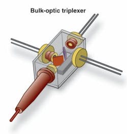
Typical FTTH networks utilize up to three wavelengths: 1490 and 1555 nm downstream to each home, and 1310 nm transmitted upstream. In some cases, particularly in Asia, only two wavelengths are used—one upstream and one downstream. In every subscriber home there is a triplexer or diplexer transceiver to manage these optical functions. The incumbent technology used for these transceivers is based on TFFs and transceiver TO-can technology (see Fig. 2). But in a market where transceiver prices are under relentless pricing pressures, PLCs have emerged as the technology of choice for replacing bulk-optic components.
These PLCs are fabricated with the same processing technology used for making electronic integrated circuits, and in some cases are even made in the same foundries. Unlike traditional bulk-optic assemblies in which light is guided through a series of lenses and filters, PLCs process optical signals through waveguides on the chip, much the same way as electrical signals are routed through an electronic integrated circuit.
Advanced wavelength filtering functions can be fabricated on the chip itself and incorporated into the regular processing steps involved with manufacturing the wafers. This approach eliminates the need for any external TFFs, greatly simplifying the subsequent assembly and packaging steps. The result is a highly integrated PLC solution, requiring no external lenses or filters of any kind. The low-cost and efficiency of this approach is greatly enhanced by the fact that all chips are made in wafer form, in which a single 6 in. silicon wafer can contain more than 500 transceiver chips.
On-chip passive and active integration
A wavelength filter alone is not enough for a full FTTH transceiver; on-chip integration of lasers and detectors is equally critical for these products. Furthermore, this integration must be done in a manner that does not sacrifice the large-scale production and high yields offered by the underlying PLC. One of the challenges faced by bulk-optic TFF diplexer and triplexer suppliers is that the alignment of lasers, detectors, and filters often requires an active process, in which all components must be powered up during assembly, adding to complexity and cost.
Modern PLC filter chips for FTTH components are designed to accommodate standard lasers and detectors on the chip, using automated passive alignment techniques. This integration is typically done with an automated flip-chip bonder capable of running 24 hours per day with very little user intervention. In the Enablence Dispersion Bridge PLC platform, alignment features for lasers and detectors are self-aligned to waveguides and gratings, patterned in the same fabrication step, and effectively lock lasers and detectors at the correct position during integration. Even transimpedance amplifier chips and associated capacitors are all mounted directly on the PLC platform, resulting in a completely self-contained FTTH transceiver chip.
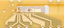
A low-cost transceiver chip must also be mated with an equally low-cost packaging solution, capable of the large volumes afforded by the PLC approach. New packaging technologies allow transceivers to be assembled and tested without sacrificing any of the reliability requirements dictated for optical networks (see Fig. 3). The development of these packaging technologies has been accomplished by leveraging many of the chip-based techniques traditionally used in microelectronics.
With the use of “multi-up” packaging technology, transceiver chips can be mounted, wirebonded, pigtailed, and even fully tested in a frame assembly consisting of nearly 20 transceivers per frame. Virtually no hands-on labor is needed, because the assembly and test systems are fully automated. Immediately before sealing the packages, the chips are encapsulated in much the same way as microelectronics chips, protecting the active components from humidity and contaminants. The result is a highly stable PLC-based transceiver platform that can operate without temperature control from -40°C to +85°C, delivering 1.25 or 2.5 gigabits of data per second.
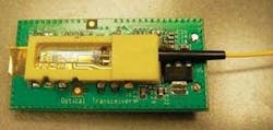
This level of integration and functionality far exceeds what PLC technology was capable of just five years ago. Chip-based integration produces a stable assembly with effectively no piece—parts that can become misaligned, making PLC technology also attractive for aerospace and defense applications in which high-vibration environments and harsh conditions are the norm (see Fig. 4). New filter technologies and PLC platforms are poised to revolutionize FTTH deployments, and will be critical in bringing optical fiber to millions of new subscribers.
Matt Pearson is vice president of technology at Enablence Technologies, 400 March Road, Ottawa, ON, Canada ON K2K 3H4; e-mail: [email protected]; www.enablence.com.