MIT nanokirigami technique creates nanoscale optical devices (with video)
Nanokirigami is based on the ancient arts of origami (making 3-D shapes by folding paper) and kirigami (which allows cutting as well as folding) but applied to flat materials at the nanoscale, measured in billionths of a meter. Researchers at the Massachusetts Institute of Technology (MIT; Cambridge, MA) and in China have for the first time applied this approach to the creation of nanodevices to manipulate light, potentially opening up new possibilities for research and, ultimately, the creation of new light-based communications, detection, or computational devices.
RELATED ARTICLE: Kirigami thin-film photovoltaic cells flex to track the sun
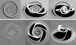
The findings are described in the journal Science Advances by MIT professor of mechanical engineering Nicholas X Fang and five others. Using methods based on standard microchip manufacturing technology, Fang and his team used a focused ion beam to make a precise pattern of slits in a metal foil just a few tens of nanometers thick. The process causes the foil to bend and twist itself into a complex three-dimensional (3D) shape capable of selectively filtering out light with a particular polarization.
Previous attempts to create functional kirigami devices have used more complicated fabrication methods that require a series of folding steps and have been primarily aimed at mechanical rather than optical functions, Fang says. The new nanodevices, by contrast, can be formed in a single folding step and could be used to perform a number of different optical functions (see video):
For these initial proof-of-concept devices, the team produced a nanomechanical equivalent of specialized dichroic filters that can filter out circularly polarized light that is either right-handed or left-handed. To do so, they created a pattern just a few hundred nanometers across in the thin metal foil; the result resembles pinwheel blades, with a twist in one direction that selects the corresponding twist of light.
"It's a very nice connection of the two fields, mechanics and optics," Fang says. The team used helical patterns to separate out the clockwise and counterclockwise polarized portions of a light beam, which may represent "a brand new direction" for nanokirigami research, he says.
The technique is straightforward enough that, with the equations the team developed, researchers should now be able to calculate backward from a desired set of optical characteristics and produce the needed pattern of slits and folds to produce just that effect, Fang says.
These devices are orders of magnitude smaller than conventional counterparts that perform the same optical functions, so these advances could lead to more complex optical chips for sensing, computation, or communications systems or biomedical devices, the team says.
For example, Fang says, devices to measure glucose levels often use measurements of light polarity, because glucose molecules exist in both right- and left-handed forms which interact differently with light. "When you pass light through the solution, you can see the concentration of one version of the molecule, as opposed to the mixture of both," Fang explains, and this method could allow for much smaller, more efficient detectors.
Circular polarization is also a method used to allow multiple laser beams to travel through a fiber-optic cable without interfering with each other. "People have been looking for such a system for laser optical communications systems" to separate the beams in devices called optical isolaters, Fang says. "We have shown that it's possible to make them in nanometer sizes."
SOURCE: MIT; http://news.mit.edu/2018/kirigami-inspired-technique-manipulates-light-nanoscale-0706
About the Author

Gail Overton
Senior Editor (2004-2020)
Gail has more than 30 years of engineering, marketing, product management, and editorial experience in the photonics and optical communications industry. Before joining the staff at Laser Focus World in 2004, she held many product management and product marketing roles in the fiber-optics industry, most notably at Hughes (El Segundo, CA), GTE Labs (Waltham, MA), Corning (Corning, NY), Photon Kinetics (Beaverton, OR), and Newport Corporation (Irvine, CA). During her marketing career, Gail published articles in WDM Solutions and Sensors magazine and traveled internationally to conduct product and sales training. Gail received her BS degree in physics, with an emphasis in optics, from San Diego State University in San Diego, CA in May 1986.
