Graphene sandwich creates ultrathin photodetector
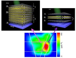
The Center for Integrated Nanostructure Physics, within the Institute for Basic Science (IBS) in Korea has developed the world's thinnest photodetector. With a thickness of just 1.3 nm—10 times smaller than standard silicon photodiodes—this device could be used in Internet of Things (IoT), smart devices, wearable electronics, and photoelectronics. This 2D technology, described in Nature Communications, uses molybdenum disulfide (MoS2) sandwiched in graphene.
RELATED ARTICLE: 'World's thinnest lens' made from layers of molybdenum sulfide
Graphene is conductive, thin (just one-atom thick), transparent, and flexible. However, since it does not behave as a semiconductor, its application in the electronics industry is limited. To increase its usability, IBS scientists sandwiched a layer of the 2D semiconductor MoS2 between two graphene sheets and put it over a silicon base. They initially thought the resulting device was too thin to generate an electric current but, unexpectedly, it did. "A device with one-layer of MoS2 is too thin to generate a conventional p-n junction, where positive (p) charges and negative (n) charges are separated and can create an internal electric field. However, when we shine light on it, we observed high photocurrent. It was surprising! Since it cannot be a classical p-n junction, we thought to investigate it further," explains YU Woo Jong, first author of this study.
To understand what they found, the researchers compared devices with one and seven layers of MoS2 and tested how well they behave as a photodetector, that is, how they are able to convert light into an electric current. They found that the device with one-layer MoS2 absorbs less light than the device with seven layers, but it has higher photoresponsitivity. "Usually the photocurrent is proportional to the photoabsorbance, that is, if the device absorbs more light, it should generate more electricity, but in this case, even if the one-layer MoS2 device has smaller absorbance than the seven-layer MoS2, it produces seven times more photocurrent," describes Yu.
Why is the thinner device working better than the thicker one? The research team proposed a mechanism to explain why this is the case. They recognized that the photocurrent generation could not be explained with classical electromagnetism, but could be with quantum physics. When light hits the device, some electrons from the MoS2 layer jump into an excited state and their flow through the device produces an electric current. However in order to pass the boundary between MoS2 and graphene, the electrons need to overcome an energy barrier (via quantum tunnelling), and this is where the one-layer MoS2 device has an advantage over the thicker one.
Because the device is transparent, flexible, and requires less power than the current 3D silicon semiconductors, it could accelerate the development of 2D photoelectric devices, say the researchers.
SOURCE: Institute for Basic Science; https://www.ibs.re.kr/cop/bbs/BBSMSTR_000000000738/selectBoardArticle.do?nttId=13809&pageIndex=1&searchCnd=&searchWrd=
About the Author

Gail Overton
Senior Editor (2004-2020)
Gail has more than 30 years of engineering, marketing, product management, and editorial experience in the photonics and optical communications industry. Before joining the staff at Laser Focus World in 2004, she held many product management and product marketing roles in the fiber-optics industry, most notably at Hughes (El Segundo, CA), GTE Labs (Waltham, MA), Corning (Corning, NY), Photon Kinetics (Beaverton, OR), and Newport Corporation (Irvine, CA). During her marketing career, Gail published articles in WDM Solutions and Sensors magazine and traveled internationally to conduct product and sales training. Gail received her BS degree in physics, with an emphasis in optics, from San Diego State University in San Diego, CA in May 1986.
