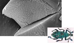
Beetles can teach engineers how to self-assemble large, high-quality 3D photonic crystals
Familiar to Laser Focus World readers, optical materials from the natural world (see related articles) can come in the form of metamaterials, photonic crystals, antireflection coatings, and many other forms. Now, researchers at Yale University (New Haven, CT), Nanyang Technological University (Singapore), University of Oxford (Oxford, England), CSIRO Ecosystem Sciences (Canberra, Australia), and Argonne National Laboratory (Argonne, IL) have discovered that some beetles produce large volumes of high-quality 3D periodic nanostructures of the type needed for some leading-edge uses in photonics.1
RELATED: Biomimetic pigmant-free polymers may aid the fight against counterfeiting
RELATED: BIOMIMETICS: Optical biomimetics emerge from a deep, dark past
RELATED: Wood-derived cellulose nanocrystals form iridescent film for textile and security applications
The team used high-intensity X-rays from the Advanced Photon Source at Argonne National Laboratory to investigate color-producing nanostructures within hair-like structures that cover some species of butterflies, weevils and beetles, bees, and spiders and tarantulas. They found that the architectures of these nanostructures are identical to chemical polymers engineered by chemists and materials scientists.
Engineers, however, have had difficulty organizing these polymers in structures large enough to make them commercially feasible, using either bottom up (self-assembly) or top-down (lithographic templates, etc.) techniques.
"These biophotonic nanostructures have the same shapes commonly seen in blends of large, synthetic, Lego-like molecules called block copolymers, developed by chemists," says lead author Vinod Saranathan, former Yale graduate student and now faculty member at Yale-NUS College in Singapore.
However, the beetles and their colleagues are already producing these structures in larger volumes using self-assembly. Learning how to imitate the beetles' technique could lead to commercialization of such structures for use in cosmetics and paints, as well as photovoltaic cells and other photonic devices.
Source: http://news.yale.edu/2015/05/14/within-colors-bees-and-butterflies-optical-engineer-s-dream-realized
REFERENCE:
1. Vinodkumar Saranathan et al., Nano Letters (2015); DOI: 10.1021/acs.nanolett.5b00201
About the Author
John Wallace
Senior Technical Editor (1998-2022)
John Wallace was with Laser Focus World for nearly 25 years, retiring in late June 2022. He obtained a bachelor's degree in mechanical engineering and physics at Rutgers University and a master's in optical engineering at the University of Rochester. Before becoming an editor, John worked as an engineer at RCA, Exxon, Eastman Kodak, and GCA Corporation.

