Efficient nanolaser is built from three-atom-thick semiconductor sheet
Scientists at the University of Washington (Seattle, WA) have built a new nanometer-sized laser or nanolaser using the thinnest semiconductor available today that is energy efficient, easy to build, and compatible with existing electronics.
RELATED ARTICLE: Electrically pumped nanolaser works at room temperature
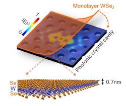
To meet modern needs in computation, communications, imaging and sensing, scientists are striving to create ever-smaller laser systems that also consume less energy. The UW nanolaser, developed in collaboration with Stanford University, uses a tungsten-based semiconductor only three atoms thick as the “gain material” that emits light. The technology is described in a Nature paper.
Other nanolaser designs use gain materials that are either much thicker or that are embedded in the structure of the cavity that captures light. That makes them difficult to build and to integrate with modern electrical circuits and computing technologies. The UW version, instead, uses a flat sheet that can be placed directly on top of a commonly used optical cavity, a tiny cave that confines and intensifies light. The ultrathin nature of the semiconductor--made from a single layer of a tungsten-based molecule--yields efficient coordination between the two key components of the laser.
The UW nanolaser requires only 27 nW to kickstart its beam, which means it is very energy efficient. Other advantages of the UW team’s nanolaser are that it can be easily fabricated, and it can potentially work with silicon components common in modern electronics. Using a separate atomic sheet as the gain material offers versatility and the opportunity to more easily manipulate its properties.
"You can think of it as the difference between a cell phone where the SIM card is embedded into the phone versus one that's removable," said co-author Arka Majumdar, UW assistant professor of electrical engineering and of physics. "When you're working with other materials, your gain medium is embedded and you can’t change it. In our nanolasers, you can take the monolayer out or put it back, and it's much easier to change around," he said.
The researchers hope this and other recent innovations will enable them to produce an electrically driven nanolaser that could open the door to using light, rather than electrons, to transfer information between computer chips and boards. The recently proven UW nanolaser technology is one step toward making optical computing and short distance optical communication a reality.
Next steps include investigating photon statistics to establish the coherent properties of the laser’s light. Co-authors are John Schaibley of the UW, Liefeng Feng of the UW and Tianjin University in China, Sonia Buckley and Jelena Vuckovic of Stanford University, Jiaqiang Yan and David G. Mandrus of Oak Ridge National Laboratory and the University of Tennessee, Fariba Hatami of Humboldt University in Berlin and Wang Yao of the University of Hong Kong.
Primary funding came from the Air Force Office of Scientific Research. Other funders include the National Science Foundation, the state of Washington through the Clean Energy Institute, the Presidential Early Award for Scientists and Engineers administered through the Office of Naval Research, the U.S. Department of Energy, and the European Commission.
SOURCE: University of Washington; http://www.washington.edu/news/2015/03/23/uw-scientists-build-a-nanolaser-using-a-single-atomic-sheet/
About the Author

Gail Overton
Senior Editor (2004-2020)
Gail has more than 30 years of engineering, marketing, product management, and editorial experience in the photonics and optical communications industry. Before joining the staff at Laser Focus World in 2004, she held many product management and product marketing roles in the fiber-optics industry, most notably at Hughes (El Segundo, CA), GTE Labs (Waltham, MA), Corning (Corning, NY), Photon Kinetics (Beaverton, OR), and Newport Corporation (Irvine, CA). During her marketing career, Gail published articles in WDM Solutions and Sensors magazine and traveled internationally to conduct product and sales training. Gail received her BS degree in physics, with an emphasis in optics, from San Diego State University in San Diego, CA in May 1986.
