OPTICAL ASSEMBLIES: Light comes to the computer chip
DAVID R. ROLSTON
For nearly 20 years, optical technologists have looked forward to the day when optical waveguides could replace the copper wire inside computing systems. But copper has performed well and remained low-cost, to the extent that various working groups are now specifying the electrical characteristics for 10 Gbit/s operation over 10 and 15 m lengths of twisted-pair copper cables.
While it is possible to reach high speeds with all-electrical technologies, however, the power required to implement the necessary interconnects is becoming exponentially more expensive. Most serial 10 Gbit/s electrical links require compensation techniques such as equalization, clock-data recovery, and pre-emphasis, not to mention better controlled material characteristics and printed-circuit-board (PCB) manufacturing. So if the trend of increased computing power at stable prices continues, the migration of optics into these systems will have to occur—and soon.
Compute and storage networks incorporate substantial multimode optical-transceiver technology, but their total power and cost is determined largely by the nonoptical "inside-the-box" technologies. The typical approach of using electrical signaling within the box and converting to optical signals at the faceplate (using pluggable optics in small form factors) to extend reach is approaching a density and power-consumption bottleneck. A large portion of the electrical energy needed for more than 10 Gbit/s serial communications goes to the circuits to maintain signal quality through the PCBs, connectors, and solderable components. And up to 30% of the total power used by the compute nodes or switches goes to the optical-transceiver modules.
Fits right in
The most cost-effective transition to optical operation is to bring light to the microchip without changing the chip. Reflex Photonics' "Light on Board" approach requires optics neither inside the microchip (no silicon ridge waveguides, for instance) nor within the printed-circuit board (for example, no embedded optical polymer waveguides). In fact, all aspects of assembly and production for the optical package are completely compatible with the standard manufacturing principles of IC packaging and PCB board population. Furthermore, it enables low total system power and high data rate (limited only by the speed of the microchip) because no "extra" electrical compensation circuitry is needed to drive transmission lines at 10 Gbit/s along a copper trace.
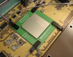
The approach places optical input/output (I/O)—in addition to the existing electrical I/O—within millimeters of the microchip. In the case of typical, large, ball-grid array (BGA) IC packages, the optical modules are placed on the top surface around the perimeter, essentially occupying the "unused" area around the microchip package (see Fig. 1).
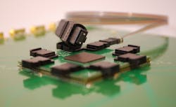
Parallel optical fiber ribbon cable, terminated in multiterminal optical connectors, enables connection either between the optical ports of IC packages or to the front panel of the box (see Fig. 2).
Simply providing optical ports around a microchip is not enough of an incentive for microchip and system architects to take advantage of the concept, however. To convince the semiconductor industry to embrace the approach, the data rate and the number of channels must provide an enormous increase over standard electrical methodologies, and cost must be competitive. Current technology can provide for more than 1500 electrical solder ball connections on a 45 × 45 mm IC package, and data rates can be upward of 2 Gbit/s per signal line (advanced BGA packages have exceeded 700 Gbit/s aggregate between processor chip and memory). And large BGA IC packages typically cost "a penny a pin," which makes a 1500 BGA package cost about $15 for assembly and test (not including the cost of the microchip).
The optical module
Inexpensive while offering high density and speed, the Reflex LightABLE optical module is an example of just such an assembly (see Fig. 3).
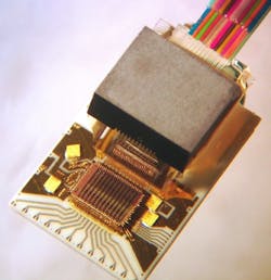
It is based on a 45° beveled front-face that can carry an M x N array of optical fibers in an area less than 1 × 2 cm. The module is mounted on an IC package near the microchip using normal packaging methods such as wirebonding or solderable surface mounting. It provides a multiterminal optical interface to which parallel optical fiber ribbons can connect. By placing eight of these modules around a microchip, each with a 2 × 12 array of optical fibers, it is possible to reach a total of 192 optical fibers. At 10 Gbit/s per optical fiber, this delivers nearly 2 Tbits per second as additional I/O that can propagate longer distances, in addition to the electrical-only I/O of the BGA package.
The optical module is composed of three portions: an optical ferrule, a microlens array, and an optoelectronic carrier. The optical ferrule is made up of a silicon V-groove chip with a 1 × 12 array of optical fibers, a precision thickness glass spacer, and a lower glass V-groove chip with a second 1 × 12 array of optical fibers. The front end of the optical ferrule is polished at 45° so the lower 1 × 12 array of optical fibers protrudes axially farther than the upper 1 × 12 array. This allows optical access through the bottom portion of the glass V-groove chip to the tips of all fibers. The optical ferrule's back end can terminate in a 2 × 12 multiterminal interface, a pig-tail, or two 1 × 12 optical-fiber ribbons. The 2 × 12 array of optical fibers within the silicon V-groove assembly has a pitch of 0.25 mm in the x-axis and 0.35 mm in the y-axis.
The optical ferrule is aligned over a three-lens optical relay system arranged as three 2 × 12 arrays of diffractive (or refractive) microlenses with diameters of 0.25 mm and pitches of 0.25 mm, and 0.35 mm in x and y, respectively, so that they are in contact but do not overlap each other. The three-lens array is formed by stacking and aligning two precision-thickness glass plates, wherein the first plate has a 2 × 12 pattern of lenses on the bottom and the second plate has two 2 × 12 patterns of lenses aligned over each other. The lens arrays are then positioned over the optoelectronic array—typically an array of vertical-cavity surface-emitting lasers (VCSELs) or photodetectors—that has been die-attached and wirebonded to a ceramic carrier plate with thin-film gold traces. The dimensions of the module are roughly 1 × 1.5 × 4 mm.
Inside the three-lens array
The three-lens array system captures the light from each VCSEL and directs it to the center of each respective optical core at the beveled optical fiber tips (see Fig. 4).
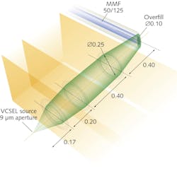
The optical path begins with a standard 850 nm VCSEL laser with 1/e2 full-divergence angle of 30°. The 3ω full-divergence angle (of a multimode VCSEL) is 45° (that is, a half-divergence angle of 22.5°) in air. Using the 3ω beam for the optical design prevents optical crosstalk into neighboring lenses.
The first lens is weakly focusing with a focal length of 0.300 mm, and is placed 0.170 mm above the VCSEL aperture. From the beam expansion of the VCSEL, the 3ω spot that is incident on the first lens is 0.15 mm in diameter (allowing for a 9 µm VCSEL aperture) and requiring an f-number of 2. The weakly focused light travels 0.2 mm through glass, where it diverges to 0.20 mm diameter (slightly less than the lens diameter) at the second lens.
The second lens collimates the light with a focal length of 0.500 mm and f-number of 2.5. The collimated light travels through 0.4 mm of glass and reaches a third lens, which has a focal length 0.500 mm and an f-number of 2.5. This focuses the light at a point 0.700 mm beyond the third lens. However, the center of the core of the beveled 45° optical fiber tip is placed at 0.350 mm above the third lens so the light overfills the 50 µm multimode core with a 100-µm-diameter spot. This results in some light loss, but allows for some lateral misalignment tolerance while still achieving a uniform coupling in all optical fibers.
A similar lens system is also possible for the upper optical fiber array, as well as the photodetector version of the module.
With multicore CPUs driving the processing capabilities within microprocessors, and with network switching speeds and interconnect data rates continuing to climb (with 10 Gigabit Ethernet and 100 Gigabit Ethernet on the horizon), optical interconnects within the box are inevitable. And with total power consumption now a critical metric in the operation and cost of such networks, optical interconnects to the chip are necessary.
The optical engineer's dream is finally poised to become reality.
David R. Rolston is cofounder, vice president, and CTO of Reflex Photonics, 550 Sherbrooke St. West, Montreal, Quebec, Canada, H3A 1B9; [email protected], www.reflexphotonics.com.