Confocal Microscopy for Industrial Applications: Microscopy reveals effects of micro-electric discharge machining on stainless steel
CHRISTOPHER A. BROWN, JOYCE M. HYDE, and JONATHAN MONTGOMERY
In the micro-electric discharge machining (μEDM) process, a spark bridging two electrodes, one of which is the workpiece, enables material to be machined from the workpiece. Two basic components make up the value added to a workpiece by μEDM: form and surface finish.
Understanding the correlations between processing parameters and surface finish, or topography, is important for the improvement of process design and process control. The relation between process variables and surface topography can be used to improve both process design and control, helping to better control the characteristics of a product by controlling μEDM parameters.
In order to examine the relation between μEDM and the surface topography of stainless steel, a stainless-steel surface can be measured using a laser scanning confocal microscope. These measurements can then be characterized with conventional parameters and parameters from multiscale areal fractal analysis (measurements from confocal microscopes are sufficiently precise for this, with surface features greater than 500 nm laterally clearly discernible). In addition, multiscale analyses indicate at what scales discrimination and strong correlations are possible. This work can also assist in advancing the understanding of the fundamental mechanisms involved in μEDM.
The objective of this case study was to investigate the relation between the energy for μEDM of stainless steel and the resulting surface topography, in particular the correlations between topographic characterizations (ASME B46.1) and machining energy. This work also examined the application of laser scanning confocal microscopy for the measurement and graphic representation of surfaces formed by μEDM and addressed the importance of scale in surface measurement and characterization.
Methodology
A laser scanning confocal microscope (LEXT OLS4000; Olympus, Tokyo, Japan), was used to measure the topographies of surfaces created using a μEDM machine (GM703; SmalTec International, Lisle, IL) at different discharge energies. These measurements were then analyzed through the use of multiscale, areal, and complexity analyses. Correlations between energy and relative area and between energy and area-scale complexity were tested using linear regression analyses at many different scales. The strengths of the correlations were then analyzed to discern any trends with respect to scale. The correlations between discharge energies and conventional height parameters were also tested, as were the correlations with smooth-rough crossovers (SRCs). The latter were calculated from area-scale analysis (outlined below).
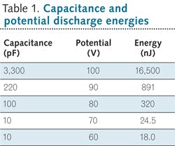
Surfaces were created on 316L stainless steel using μEDM technology based on a resistive-capacitive circuit system in which different discharge-pulse energies are selected by the size of the capacitor in the circuit. If the system fully discharges and recovers before discharging again, the theoretical energy generated is as given in Table 1. This energy determines the maximum material removal rate. The values used in this study represent the most common energies used when manufacturing μEDM parts. The tool electrode was formed by pulling a 99.99% tungsten wire with a 3000 rpm spinning mandrel cylinder. The μEDM energy levels used for this study are listed in Table 1, which illustrates that higher capacitance produces a lower natural frequency for the circuit and creates a more energetic discharge.
The μEDM-machined surfaces were measured using the LEXT OLS4000, with all measurements made with a 100X objective lens with a numerical aperture (NA) of 0.95 and a 405 nm wavelength laser. Each surface was measured four times over a region of 128 × 128 μm, collecting a 1024 × 1024 sampling of elevations in each measurement. The sampling interval was approximately 125 nm when no zoom was used (surfaces were measured with no zoom for the analyses). All surfaces were also observed with a 100X objective with zoom of 8X, resulting in the observation of a 16 × 16 μm region with a sampling interval of approximately 16 nm.
Surface measurements were processed using form removal and modal outlier filtering. Conventional height parameters were also determined. Area-scale and complexity-scale analyses (ASME B46.1 2009, ISO 25178-2 2012)1 were performed on the filtered files. Relative surface areas were evaluated over the areal scales available in the measurement, from half the region measured (8192 μm2) to half the square of the sampling interval (0.0078 μm2).
The correlations of the relative areas and the area-scale fractal complexities were determined using linear regressions at each of the analyzed scales. Regression coefficients (R2) were determined from linear regression analyses when performed on conventional height parameters and SRCs with respect to discharge energies.
Results
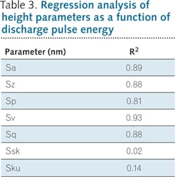
Images rendered from surface measurements created at the highest energy μEDM (16,500 nJ) are shown in Figures 1(a) and 1(b) (no zoom and 8X zoom, respectively). What appear to be craters formed by discharge pulses can be seen as visible depressions in Fig. 1(a) (crater diameter is ~10 μm). The image created with 8X zoom, as shown in Fig. 1(b), features a distinct ridge that shows the limits of the crater. The ridge is a few hundred nanometers in width and slightly less in height. Inside the crater, few features are visible and the surface is relatively smooth with a few small bumps and waves.Areal height parameters-including peak-to-valley height (Sz), peak height (Sp), and valley depth (Sv); the arithmetic average roughness (Sa) and root mean square roughness (Sq); and the skew (Ssk) and kurtosis (Sku)are listed in Table 2. Height parameters and average heights all tended to increase with increasing μEDM energy. Skew and kurtosis did not appear to show any clear trend. A regression analysis for these same parameters is shown in Table 3; the strongest correlation is the valley depth with a regression coefficient (R2) of 0.93.
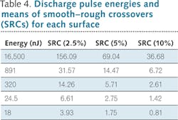
Table 4 shows the mean SRCs for all energies. SRCs were computed using thresholds in relative areas based on 2.5%, 5%, and 10% of the greatest relative area calculated for that surface (ASME B46.1 2009). Within all thresholds, SRCs increased steadily with discharge-pulse energies.
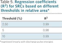
The R2s for linear regression of SRCs are shown in Table 5. All three thresholds provide SRCs that have regression coefficients greater than 0.98, which are significantly stronger than the regressions with conventional height parameters.
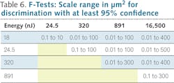
The ability to discriminate between μEDM-machined surfaces with 95% or greater confidence (F-Test) is summarized in Table 6. The SRC for the relative area versus scale graphs for each energy surface was somewhat lower than the maximum scale for discrimination.
Conclusions
Laser scanning confocal microscopy can be used to precisely measure the topographies of stainless-steel surfaces machined by μEDM with different discharge-pulse energies to scales of 200 nm laterally and tens of nanometers vertically.
For the μEDM-machined surfaces measured with confocal microscopy in this study, height/texture characterization parameters correlate well with discharge-pulse energies (the R2 values are between 0.81 and 0.93), while skew and kurtosis do not correlate well with discharge-pulse energies (the R2 values are <0.15). The relative area and the area-scale fractal complexities are able to discriminate their surfaces with greater than 95% confidence over a minimum range in scale between 0.1 and 10 μm2 up to a range of 0.01 and 500 μm2.
The strongest correlations were found using multiscale areal analysis: the SRCs correlate with the discharge-pulse energy with R² values of 0.98 and 0.99. The relative area correlates with the discharge-pulse energy with an R2 = 0.98 between scales of 10 and 100 μm2; the complexity correlates with the discharge-pulse energy with an R2 = 0.97 between scales of 100 and 200 μm2.
Summary
Several types of features consistent with known EDM mechanisms are discernible on images rendered with the LEXT OLS4000 on surfaces created by μEDM. The measured surfaces created with different pulse energies can be discriminated clearly over wide ranges of scales using area-scale analysis. Strong correlations were found between the discharge-pulse energies with which the surfaces were created and calculated texture-characterization parameters. The strongest correlations were found with the SRC scales, the relative area, and the area-scale fractal complexity.
The microscopic measurements of the μEDM-machined surfaces showed a variety of features, including what appeared to be overlapping craters resulting from localized melting and evaporation by the discharges, as well as solidified crater boundaries and crater interiors. Multiscale areal analysis elucidated the differences and similarities among the surfaces over a wide range of scales.
Laser scanning confocal microscopy stands to assist in fine-tuning the μEDM process to create surfaces tailored toward specific applications.
Acknowledgments
The authors would like to thank the following: Olympus for providing the LEXT OLS4000 laser scanning confocal microscope; SmalTec for providing the μEDM-machined surfaces; and Surfract, owned by coauthor Christopher Brown, for providing the software for area-scale and complexity scale analyses and the correlation analyses and discrimination tests. Additional special thanks go to Lionel Cadet of the École Nationale d'Ingènieurs de Saint-Étienne, a visiting student in the Surface Metrology Lab at WPI, who did the excellent measurement work.
The original article on which this case study is based is to be published in the academic journal Surface Topography Metrology and Properties.
Reference
1. ASME B46.1-2009 Surface Texture (Surface Roughness, Waviness and Lay), American Society of Mechanical Engineers.
Christopher A. Brown ([email protected]) is a professor of mechanical engineering and director of the Surface Metrology Lab at Worcester Polytechnic Institute (WPI; Worcester, MA). Joyce M. Hyde is also at the Surface Metrology Lab at WPI. Jonathan Montgomery is a research and development engineer at SmalTec International (Lisle, IL).
