SCANNING OPTICS: Optical-sectioning microscope uses a single-pixel detector
Confocal microscopy, in which the image of a point source is scanned across the specimen and the collected light filtered by a pinhole to block the out-of-focus light, allows a 3D image of the specimen to be built up point by point—a valuable property for both science and industry. In the latter, the technique is widely used to image and inspect the patterns manufactured on semiconductor chips.
The scanning in an ordinary confocal microscope (CM) requires a mechanically moving stage or other device to move the focal spot relative to the specimen. In contrast, a programmable-array microscope (PAM) contains, somewhere within its optical train, an array with pixels that can be switched on and off in individual sequence to mimic a mechanically scanned point of light. The array can be a digital-micromirror device (DMD), liquid-crystal-on-silicon (LCoS), or other type of 2D programmable array; such devices usually allow scanning at kilohertz rates. A PAM also requires a second 2D imaging array precisely aligned to the final image of the programmable array.
Compressive sensing
The complexity of the PAM optical system has led researchers at the University of Delaware (Newark, DE) to simplify things by applying a technique called compressive sensing (CS), in which many pixels on the programmable array are switched on at the same time in different predetermined patterns and all the light from the specimen collected at once; subsequent calculations derive the image from the results.1 Using CS allows the second array (the 2D imaging array) to be eliminated and a single detector to be used instead.
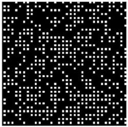
The pixel patterns for CS must be carefully designed so that they efficiently collect the data for the subsequent calculations; each pattern must have no two adjacent pixels on at the same time; and in combination the patterns should include every pixel of the array. The researchers chose to use patterns called modified scrambled-block Hadamard ensembles (see figure).
Design and model
In the experimental single-pixel (SP) PAM system, light from an incoherent (tungsten-halogen) illumination source is introduced to a DMD programmable array via a beamsplitter and a relay lens; the illumination intensity across the array is approximately uniform. The DMD is in turn imaged onto the specimen via a collimating lens and a microscope objective with 40X magnification and a numerical aperture (NA) of 0.65. Light collected from the specimen takes the path back through the system, passing through the beamsplitter to a single-pixel detector.
The DMD has frame rates of up to 8000 frames per second. Each micromirror in the DMD has an off position of -12° and an on position of 12° from the normal of the DMD; as a result, the illumination light for the SP-PAM is introduced at 24° from the normal so that the mirrors reflect the light at 0° when in the "on" state.
The researchers modeled a simplified version of their system with an optical-design program to examine the transfer functions of versions of the PAM architecture with differing parameters. They concluded that a smaller DMD pitch (relative to the illumination wavelength) results in a more-widespread transfer function, meaning a narrower impulse response and thus a smaller single-pixel illumination size on the image and better resolution. In addition, they found that the transfer functions had some so-called blind spots, which could mean that the DMD-based SP-PAM does not resolve some spatial-frequency components.
Discerning texture
The researchers used the SP-PAM to generate 2D optical sections of a dry-etched silicon sample. The sample had etched holes about 8 µm deep with rough sidewalls and bottom surfaces; the sample itself was tilted slightly with respect to the image plane due to a tilt in the sample stage. In addition to optical sections, a "control" image was taken with the single-pixel detector replaced with a CCD array and with all the DMD mirrors turned on.
The neighboring sections were 2 µm apart from each other along the optical axis. When compared to the control image, the optical sections show more contrast between the rough and smooth portions of the sample, thus better revealing the variations in surface texture.
Gonzalo Arce, one of the researchers, notes that for finer resolution, higher-NA objective lenses can easily be used in the setup. "In terms of the next step in the experimental setup, we plan to extend the current single-path architecture to a dual-path compressive confocal architecture," he says. "In a single-path mode, we use the conjugate image only. The dual-path compressive confocal microscope (CCM) exploits both the conjugate and the nonconjugate images. The dual-path CCM, in theory, allows us to simultaneously reach signal-to-noise-ratio values and acquisition times that are not possible with other existing confocal microscopy systems. In addition, we are modifying a scientific-grade microscope into a CCM system. This upgrade will give us more-convenient interfaces to different objective lenses, better optical-alignment accuracy, lower noise contamination, and a more rigid system construction."
REFERENCE
- Y. Wu et al., "A single-pixel optical sectioning programmable-array microscope," SPIE Photonics West 2010, Conference 7596, Jan. 27, 2010.
About the Author

John Wallace
Senior Technical Editor (1998-2022)
John Wallace was with Laser Focus World for nearly 25 years, retiring in late June 2022. He obtained a bachelor's degree in mechanical engineering and physics at Rutgers University and a master's in optical engineering at the University of Rochester. Before becoming an editor, John worked as an engineer at RCA, Exxon, Eastman Kodak, and GCA Corporation.