SPECIALTY FIBER: Fiber lasers lower cost of making SAWs
AJAY PATEL, BRIAN LINCOLN, and DREW STONE
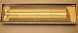
Surface-acoustic-wave (SAW) devices and modules are widely used in precision electronic components such as modulators, transducers, and filters used in the defense and aerospace industries (see Fig. 1). The demanding military requirements for these devices can create challenges for many of the key manufacturing steps in the production chain.
Among the numerous critical processes involved in the production of SAW components is the manufacturing of phase-correction masks, which take the form of metallic film patterns. This manufacturing process traditionally relied on a solid-state laser to cut foil shadow masks, as this enabled arbitrary mask profiles and clean-cut edges. However, fiber lasers have recently become the preferred laser systems for the cutting process, bringing the benefits of increasing throughput, improving cutting quality, and lowering overall process costs.
SAW device manufacturing
Phonon Corp. makes SAW devices for the defense and aerospace industries, including filters, delay lines, oscillators, and higher-level modules for high-performance radio-frequency (RF) signal processing. Surface-acoustic-wave techniques using linear bandpass filters or delay lines allow the synthesis of arbitrary amplitude and phase, defined by linewidth and substrate size.
A common device is the dispersive filter, or delay line, which consists of linear filters with group delay that varies by some finite period over the passband. The impulse response of this device is a frequency-modulated (FM) pulse whose instantaneous frequency varies by its passband over its duration. The FM is usually chosen to be linear (LFM), with the amplitude response being flat or weighted to suppress side lobes. Nonlinear FM (NLFM) can also be implemented, the tradeoff being improved signal-to-noise vs. greater Doppler sensitivity.
Several techniques are available to manufacture such filters: All consist of varying the propagation path length with frequency. One design uses a reflective-array compressor (RAC)—by far the dominant technique for creating larger dispersive durations. The device is made using a piezoelectric substrate (often quartz or lithium niobate) and is usually heated because of the frequency-temperature characteristics of the substrates.
Lithography produces two short transducers and the RAC, which obtains dispersion using two long oblique acoustic reflector arrays that are frequency-selective due to their nonuniform period. The RAC design allows post-photolithography phase-error correction by insertion of a metallic film pattern between the arrays, the masks for which are cut using a laser system.
To manufacture these devices, Phonon has a 2000-sq-ft wafer fabrication facility and a 5000-sq-ft component assembly facility. Post-sealed components are built into module subsystems in a module assembly facility, and both electrical and environmental testing of components and modules is done in-house.
To make SAW devices, 3 and 4 in. substrates are first cleaned and patterned using specific photoresist exposures and a SAW photomask, followed by aluminum metallization deposition in a vacuum evaporator. Liftoff is performed to remove unwanted metallization using a solvent bath. The completed wafer yields from 1 to 200 die.
Substrates then move to component assembly, where the back of the substrate is sandblasted, etched to disperse unwanted reflection, and diced into individual die. It is at this time that, through a process called "auto-dispense," an absorber material is precisely deposited onto the die to absorb unwanted reflections. Technicians assemble die into packages and wire-bond according to controlled build instructions. Concurrently, electrical testing may be performed to ensure proper device performance before hermetically sealing in a vacuum glove box and leak testing.
Laser marking is then performed on the devices to provide permanent identifying information such as part number, date code, and serial number. If the component is to be built into a higher-level module, additional processing and buildup occurs at module assembly. As a last step in the process, final testing of devices and modules is done using network analyzers, spectrum analyzers, environmental ovens, and other necessary test equipment.
Mask-cutting cost reductions
One of the critical processes in the manufacturing of SAW devices is the production of phase-correction masks, or shadow masks. These masks are used to create patterns on the surface of a substrate in a vacuum-deposition process by only allowing the gaseous metal to condense where openings in the mask have been created. The masks are made from steel shim stock ranging in thickness from 0.003 to 0.010 in. Each of these masks is unique, and the geometry of the desired electrode pattern is calculated to match the acoustic response of each device.
Software is used to calculate this exact pattern based on the results of an acoustic evaluation. The software exports these coordinates to a vector-file format that is then imported into Prolase laser-marking software (American Laserware; Chuluota, FL). Adding electrode metallization in these precise locations allows accurate tuning of the SAW component to give more uniform time delay over a larger range of frequencies.
For years, an industry-standard, flashlamp-pumped, 20 W Nd:YAG laser source was used in this manufacturing process. The laser was bulky—about the size of a refrigerator when including the power supplies and other electronics—and required 208 V three-phase electrical power as well as a constantly flowing source of chilled water for coolant.
Additionally, because YAG laser technology is based on several consumable components, periodic replacement of YAG rods ($2500 each) and frequent replacement of flashlamps ($150 each) was required. Performing this maintenance service operation required a trained service engineer or technician. Replacing YAG rods can be tricky, risking damage and degradation to the system. Such a repair operation necessitated laser system downtime, which reduced process capacity and interrupted manufacturing flow, making it more difficult to meet customer delivery dates.
Comparison to YAG lasers
Fiber lasers offer an alternative to YAG lasers. Based on ytterbium (Yb) doped fibers and pumped with solid-state single-emitter laser diodes emitting at 915 or 976 nm, these fiber lasers emit at 1064 nm, the same wavelength as YAG lasers. The efficiency of these pumps, from electrical current to pump light is very high, with wall-plug efficiencies often exceeding 30%. Fusion-splicing these fiber-coupled pump sources directly to the doped gain fiber allows for optimized excitation of the ions that convert the shorter pump wavelength to the desired 1064 nm light.
The conversion efficiency within the doped fiber, from pump source to optical output, is roughly 50%. Thus, fiber-laser sources are more than twice as efficient as YAG (8–10%) or CO2 (10–12%) lasers. Accessories for these Yb-doped active fibers can include matching passive and photosensitive fibers to create fiber Bragg gratings (FBGs), combiners, and other essential components necessary to build fiber laser sources. The matched fibers are designed to minimize splice losses when used with the corresponding active fiber.
In particular, Q-switched pulsed fiber lasers offer a compact, electrically efficient alternative to Nd:YAG technology. Roughly the size of a toaster (215 × 284 × 95 mm and 5.8 kg), a Q-switched pulsed fiber laser requires no preventive maintenance, runs off a standard 24 VDC power supply (less than 8 A for 20 and 30 W), and has integral air-cooling fans and an industry standard digital interface for laser operation.
For foil cutting of phase-correction masks, a 30 W Q-switched optical fiber laser was aligned to a ScanCube (ScanLab; Munich, Germany) galvo head equipped with a 330 mm f-theta lens, an RTC4 control board, and Prolase Laser Software. The new laser resulted in a cutting time of only 1 min, compared to 30–40 min using the previous YAG-based system, an increase in throughput of 3000–4000%.
The additional power and better beam quality provided cleaner cut edges and faster cutting speeds when fabricating these complex evaporation masks. The parts and labor costs associated with YAG laser maintenance were eliminated, saving about $5000 per year. Also eliminated were the higher costs of power consumption for both the YAG laser and the chiller, the dedicated chiller itself along with its maintenance, and the footprint of a large freezer-sized box plus chiller.
Product marking processes
This same fiber-laser system is also used for product marking and branding. Because each of the masks is unique, it is useful to engrave the SAW serial number onto the mask for easy pairing prior to metallization. This traceability increases productivity and helps eliminate waste in a product that is very near completion.
Besides marking and cutting steel, other materials that can be marked include aluminum, Kovar, and nickel and gold platings. Text characters ranging in height from 0.025 in. to greater than 1 in. can be marked on the part. Graphics, logos, symbols, and two-dimensional (2D) barcodes can also be created in the laser marking software.
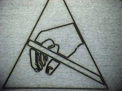
An illustration of a typically marked ESD symbol is seen in Fig. 2. This metallic cover is a nickel-plated aluminum lid used to protect the SAW device. To enhance contrast, some manufacturers prefer overexposing the metal, allowing for some amount of oxidation or burning of the metal.
Laser-marking parameters can be varied to change the appearance of the resultant marking; the results are material-dependent. By adjusting the laser power, focused spot size, pulse repetition rate, scanning speed, hatching configuration, and number of passes, many different looks can often be achieved. The key is to optimize the appearance of the marking (subjective or quantified) while achieving target-cycle times short enough to reach the desired throughput.
Laser marking systems are also used to permanently mark unique ID (UID) codes. These codes are part of the US Department of Defense (DoD) inventory-management system, which requires that all mission-critical components permanently display this mark on the product. The UID is a 2D Data Matrix code that is configured with information in a standardized format to provide traceability on each device (see Fig. 3).
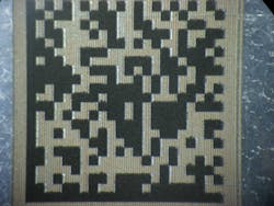
Here, the base material is a tin-lead-plated aluminum cover with a zincate and copper strike. The overall appearance of the bare cover is rather shiny, reflecting much of the light that a typical scanner would output for reading the UID. To make the UID more visible to these scanners, a thin layer of tin-lead is ablated, then marked over with the UID. The resulting effect is a finely etched and burned UID with 98% character readability, satisfying the DoD requirements.
Increasing market for low-power fiber lasers
Fiber lasers are a mature, stable technology that is rapidly replacing older laser technology in many applications. In doing so, these fiber lasers can help end users reduce their manufacturing costs. Advantages include high wall-plug efficiency, small size, air cooling, no consumables or preventative maintenance, and high reliability.
Low-power (less than 100 W) fiber lasers are excellent tools for marking, engraving, and even cutting (for thin cross-sections) most metals. Filled plastics and ceramics can also be processed with fiber lasers.
Laser-marking technology should be considered whenever permanent part marking is required. It's quicker and cleaner than chemical etching, creates no force on the part as with pin stamping, and requires no hard tooling, making it ideal for rapid prototyping or customization.
ACKNOWLEDGMENTS
Our appreciation is extended to Tom Martin, the president of Phonon, for his support, as well as to Ajay Patel for his assistance with writing this article and providing details and photographs of the processes at Phonon.
Ajay Patel is an engineer at Phonon Corp., Simsbury, CT; e-mail: [email protected]. Brian Lincoln is a sales engineer and Drew Stone is product line manager at Nufern, East Granby, CT; e-mails: [email protected] and [email protected].