NEXT-GENERATION LITHOGRAPHY: Schott shooting to be a player in nanoimprint lithography
Nearly 17 years have passed since the first instance of nanoimprint lithography hit the literature, but only now is industrial interest gathering pace—this month with glass giant Schott (Mainz, Germany) getting in the game. But their stated interest—nanoimprint lithography on glass—is somewhat different from what other industry players have been pursuing.
The technique, which goes also by the name hot embossing, involves the development of a master pattern through conventional nanolithography techniques such as electron-beam lithography. The master is then used as a stamp and pressed onto a substrate that is coated with a resist; the stamp is then heated to cure the resist. The master is removed and anisotropic etching techniques are used to transfer the pattern to the substrate.
First laid out by Stephen Chou—then at the University of Minnesota (Minneapolis, MN)—and colleagues in a landmark Science paper, the technique has been finding its way into a range of applications that leverage its attractive combination of subwavelength structure generation and high throughput.1
Since those early days, a great many laboratory demonstrations have shown off nanoimprinting’s ability to make large-area optical and electronic elements, from gratings to thin-film transistors. But it has gained ground in industry as well. Hitachi Global Storage Technologies has been investigating nanoimprint approaches for magnetic-storage applications, though it remains unclear whether the requisite feature density can be reached to entrench the technique on a wider scale.
Mentioned in ITRS
Nanoimprint techniques are also appearing in the International Technology Roadmap for Semiconductors (ITRS, a technology-assessment document produced by a team of industry experts), a vote of confidence from the semiconductor industry that suggests nanoimprinting has a strong future in electronics. In 2007, Toshiba validated the technique for the 22 nm node that the industry is currently working to.
“The clear advantage of nanoimprint is its ability to replicate patterns over large areas at higher resolution than competing methods can achieve,” says Karl Berggren, a nanolithography expert at the Massachusetts Institute of Technology (Cambridge, MA). “But it still has to get past problems of defectivity and costs associated with mask manufacturing. It only replicates patterns—someone still has to make the master pattern and that is a far from trivial challenge.”
For critical subwavelength applications in optics and electronics, this “defectivity” measure—the number of imperfect impressions, inclusions, resist nonuniformities, and other flaws—will have to be addressed. Toshiba claimed defect densities of fewer than 0.3/cm2 with 24 nm dense features, comparable to the best competing technologies at the time.
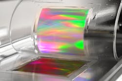
But Schott’s entry into the sphere suggests that nanoimprint could make an impression in other applications. The firm is aiming to roll-print features onto large glass substrates 30 × 40 cm in size to give the surface, for example, a custom refractive index (via a sol-gel nanoimprint coating) or the look of metal. These are just the kinds of macroscopic applications of nanoscopic features for which defectivity will be less of an issue. Schott seems poised to go further with the technique.
“We are working hard to turn nanostructuring into a technology platform for the future development of innovative applications and products,” says Eveline Rudigier-Voigt, senior manager for coatings at Schott’s research arm.
L. Jay Guo of the University of Michigan (Ann Arbor, MI) has been pursuing just this kind of large-scale, roll-to-roll nanoimprint work for a number of years and across a number of patents. “I think it represents the beginning of adoption of the technology by industry,” he says. “Though nanoimprinting has been developed for 17 years, many people have been focusing on the electronic and magnetic recording applications that have extremely stringent requirement on defectivity level. But there are plenty of other applications that are defect tolerant.”
Guo believes that Schott’s move may be the start of sharp growth of the approach, away from its solid but niche position in the electronics industry. “I think volume could be a big driver,” he notes. “People like a better and nicer living and working environment. I think once the idea is out, people will be able to come up with even more applications that many cannot foresee at this point.”
REFERENCE
1. S. Chou et al., Science, 272, 85 (1996); doi:10.1126/science.272.5258.85.