Diffractive Optics: Nanoimprint lithography enables fabrication of subwavelength optics
JIAN WANG AND HUBERT KOSTAL
With their unique properties, diffractive optics can improve optical systems by increasing their reliability, robustness, and functional integration, while reducing their effective size. One interesting class of diffractive optics has critical dimensions smaller than the wavelength of the light with which they are designed to interact. These nano-optic diffractive structures typically have grating periods ranging from 50 to 200 nm. They exhibit only zero-order diffraction, allowing for precise control of light without loss into undesired orders; with appropriate selection of materials they can exhibit, among other optical properties, form birefringence or polarizing behavior, or both simultaneously; and their optical function is realized in less than a micron of thickness. Polarization filters, polarizing beamsplitters, spectral filters, retardation plates, and lenses are among the functions that have been demonstrated using subwavelength-grating structures.
Breakthrough efficiencies in the manufacturing of these optical components must be achieved to drive down the cost of subwavelength diffractive optics. Such optics can be designed using a broad material range that includes dielectrics, metals, polymers, and plastics, and many types of regular structures, including linear, grid, and circular, which allows them to be fabricated by extending semiconductor-production techniques that simplify and reduce the cost of optical-component fabrication. Specifically, nanoimprint lithography is an emerging manufacturing methodology that simultaneously enables high-throughput wafer-scale production and the nanoscale lithographic resolution needed to produce multifunction integrated subwavelength optical components.
Nanoimprint lithography
Standard photolithography is now capable of creating sub-100-nm linewidths, but even this is not yet sufficiently high resolution to be generally usable for the creation of practical subwavelength diffraction gratings. Other lithographic approaches have been developed specifically to address these challenges, including “soft lithography” (or microcontact printing), atomic-force-microscope/dip-pen lithography, and nanoimprint lithography. Of these, nanoimprint lithography has so far demonstrated the most commercial success, both in the availability of commercial manufacturing tools and in the proliferation of subwavelength optical components now available in volume.
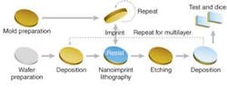
Nanoimprint lithography is distinguished from photolithography in that it uses mechanical methods-that is, contact (or “printing”) by a master mold-to deform the resist layer into a physical shape that can be used as an etching mask to realize subwavelength-scale patterns and structures (see Fig. 1). The mechanical nature of nanoimprint lithography eliminates resolution-limiting factors associated with lithography methods that depend on beams of energy, such as light diffraction or electron-beam scattering. Sub-10-nm structures have been demonstrated using nanoimprint techniques. As an added capability, because it is a mechanical technique and deforms the resist layer into a 3‑D structure, nanoimprint lithography has the unique capability to form 2-D patterns, as well as to directly form 3-D structures (which can be used to create lens arrays).
Essential attributes
The chemistry of a resist used in nanoimprint lithography must support uniform application to the substrate, be easy to shape, be capable of being set based on either thermal or UV properties, and work effectively as an etching mask. In general, this requires that the resist be of low viscosity for easy flow and patterning, that it has a fast UV-cure speed or sets at a convenient temperature (usually between 80°C and 100°C), and that it exhibits good etching properties after curing.
Because nanoimprint transfers patterns at a 1× resolution, any physical mold used in the process must be created with features scaled to the final target dimensions. The mold is created using complex, relatively time-consuming methods that are unsuitable for high-throughput production-but this approach is acceptable because the use of nanoimprint lithography allows the cost of creating the mold to be amortized across repeated applications in manufacturing. Typically electron-beam or interference lithography is used for mold creation, with the choice of method depending on the desired pattern and application. Note that the mold, once created, is reusable and can be easily replicated with nanoimprint techniques. Common materials for the mold include nickel, silicon, and glass.
Both whole-wafer (for 4- and 6-in. diameters) and step-and-repeat (usually with molds on the order of 1- to 2-in. diameter) approaches to the imprint step have been developed. Each has technical advantages, with whole-wafer patterning seeming to permit higher throughput and lower cost for simple diffraction gratings. Under either method, the pattern is created in the resist by a combination of mold pressure and capillary action.
If the function of the nanostructured layer is being positionally matched to a particular physical or optical property of the underlying substrate, alignment accuracy can become a requirement. Precise angular alignment can be achieved in whole-wafer nanoimprint, but alignment of complex structures is more precise using step-and-repeat methods.
Once the polymer is set, contact between the mold and the polymer layer must be broken without damaging the imprinted features, and without transferring any residue to the mold (which could then become an undesired part of the next pattern imprinted). The separation forces needed are highly dependent on the specific geometry of the pattern imprinted and the surface area created. This potential problem is handled in part by treating the mold with a release agent and incorporating a similar material in the resist chemistry.
Plasma etching-for example, reactive-ion etching (RIE)-methods are used to transfer the pattern from the resist to the underlying target-material layer. Matching etching speeds, accuracy, and resolution to the shape (for example, straight or tapered) and depth (from less than 50 nm up to 1 µm) is required for high throughput and yield.
Challenges
Nanoimprint lithography presents several challenges when used in commercial manufacturing, the most significant of which are defect control, end-to-end wafer processing, and throughput. A particle captured between the mold and the substrate during the imprint process can result in a much larger defect on the processed substrate than its diameter, as it will spread under the pressure of the imprinting process. In addition, a hard particle can damage the mold itself, creating a defect that will be propagated in later uses. Therefore, controlling the cleanliness of the mold and substrate, and the environment in which the imprinting is done, is critical to maintaining high yield levels.
The nanoimprint lithography operation is only one step in realizing a usable optical device. Preprocessing (including substrate cleaning and target-layer deposition), pattern transfer (via RIE), postprocessing (including deposition of protective layers and antireflection or index-matching surface coatings), and testing and dicing to size must all be integrated into an efficient manufacturing flow.
For practical purposes, the nanoimprinting step is the limiting factor in throughput (as measured by devices produced per hour of operations), as the other operations are well understood from semiconductor manufacturing and are readily scalable. Initial nanoimprint systems have demonstrated a repeatable wafer-per-hour throughput of 5% to 10% of that achieved for semiconductor manufacturing with state-of-the-art deep-UV steppers. Work is under way to reduce this gap, as well as to increase automation in wafer handling.
Advantages
Several attributes of nanoimprint lithography make it particularly intriguing for general manufacturing of optical devices. First, it is basically a semiconductor manufacturing process and therefore can be expected to realize significant economies of scale in volume production. Because the production method is the same for a broad range of potential optics, multiproduct economies of scale-say between polarizer and waveplate production-should be readily achieved, providing significant cost reductions when compared to traditional optical-component manufacturing techniques, which tend to be specialized to specific device technologies.
Second, the nanoimprint lithography process is not bounded by the requirement that an optic can only consist of a single grating structure or layer. Multifunctional optics have been demonstrated by placing subwavelength grating layers one on top of the other. Pixelated optics-devices with different optical properties arranged in a regular pattern such as an array-have been demonstrated as well; this is achieved by creating the mold through a multistep, multimask process. Both of these capabilities can be leveraged to create complex, integrated, multibeam optical devices without having to resort to epoxy bonding or other forms of lamination.
Third, nanoimprint lithography can be readily integrated with other manufacturing flows and optical or optoelectronic substrates. Functionally, a subwavelength grating structure can be thought of as a thin-film coating and can be integrated into a manufacturing flow as a wafer-processing step. Also, the nanoimprint process, aside from some requirements related to process temperature and substrate handling, is relatively “substrate agnostic,” meaning it can be applied to substrates that have already been processed in another manufacturing flow or that have an inherent optical function themselves. An example of this is applying a subwavelength polarization grating to a garnet (for example, Faraday rotator) substrate to create a very thin optical-isolator core. Similarly, the nanoimprint process separates the patterning of the resist from the pattern transfer to the underlying target material, allowing a broad range of creativity in material selection: nanoimprint lithography has been used to create diffractive gratings in dielectrics, III-V semiconductor materials, metals, polymers, and plastics selected according to the demands of the application.
Subwavelength gratings
The optical performance achieved with properly designed subwavelength gratings is comparable to that of traditional optics. However, the compact functional layer and unique behavior of nano-optic devices often allows a rethinking of optical component or system design to realize cost and performance improvements in ways that cannot be achieved with traditional optics (see Fig. 2).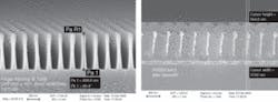
Appropriate selection of materials and grating dimensions allow subwavelength gratings to be designed and realized for operation across a broad range of wavelengths, and thus applications. Beyond communications applications, subwavelength diffractive gratings have been demonstrated for filtering in digital-imaging systems, polarization management in projection television systems, polarization management and switching in CD/DVD/Blu-Ray/HD-DVD optical drives, modulated reflective structures for ultra-high-density optical disks, signal conditioning in industrial optics applications, filters for optical sensors, and tunable optics for imaging and sensing applications.
A fundamental requirement in realizing the potential of subwavelength diffraction gratings is a high-volume, cost-effective manufacturing methodology, which is being provided by nanoimprint lithography. This combination is demonstrating initial commercial success today and has the potential to grow rapidly over the next few years.
Jian Wang is chief technical officer and Hubert Kostal is vice president of marketing and sales at NanoOpto, 1600 Cottontail Lane, Somerset, NJ 08873; e-mail: [email protected].