OPTOELECTRONIC APPLICATIONS: MICROPROCESSING: Imprint lithography challenges EUV for next-generation chip manufacturing
While the semiconductor industry is clearly committed to 193 nm photolithography and immersion lithography for chip manufacturing down to the sub-32 nm node, it is still a matter of debate as to what will happen beyond that in terms of manufacturing the increasingly fine features on silicon chips. In recent years, a number of alternative techniques have been investigated, including soft lithography, AFM/dip-pen lithography, interference lithography, and nanoimprint lithography (NIL). Of these, NIL—a mechanical process that can pattern extremely fine features onto thermoplastic substrates—has attracted the most attention, in large part because of its ability to produce very-high-resolution nanometer-scale features at less cost (about 25% lower capital expense) than extreme-ultraviolet (EUV) lithography.
In the near-term, NIL is gaining acceptance in the manufacture of optoelectronics, biotech (such as lab-on-a-chip systems), and memory/storage devices-areas in which the technology’s inherent defect issues (due to the contact nature of the process) have less impact on device performance. However, NIL proponents claim that, with proper investment by the semiconductor industry, these defect issues could be easily resolved, paving the way for NIL to become a viable chip-manufacturing tool.
“To make a technology IC-ready, you need billions of dollars,” said Stephen Chou, a leading pioneer in imprint and nanoimprint technologies and applications. “If you look at the history of conventional lithography development, each year the chip companies spend $1 billion to improve conventional technologies. Ultraviolet litho took at least $10 billion to get where it is. But so far only a few hundred million has been invested in NIL, insufficient to be IC-ready. I think NIL has tremendous potential, but to become IC-ready it needs a much bigger investment.”
The pros
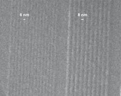
The fundamental concepts behind NIL—also known as imprint lithography—actually date back to the first printing presses, while the earliest recorded proposals for using a mechanical imprint process in microlithography were in the mid 1970s.1 The first patent related directly to ultraviolet NIL was published in 1993. In 1996, Chou—generally considered the “father” of NIL, having coined the terms “imprint lithography” and “nanoimprint lithography”—and colleagues at the University of Minnesota demonstrated 25 nm feature resolution on a polymethyl methacrylate (PMMA) substrate using NIL.2 More recently, his group demonstrated 10-nm-resolution features with NIL (see Fig. 1).
“About 15 years ago I recognized that if you could make the feature size of the optical device smaller than the wavelength of light, this would enable a new class of devices,” said Chou, now professor of engineering and head of the NanoStructure Laboratory at Princeton University (Princeton, NJ). “About 13 years ago, I recognized if we didn’t develop some cheap manufacturing technology, the field of nano would stop, and this is what led to NIL. My philosophy from the beginning has been very simple: we must make the device size smaller than the limits of physical scales, which would allow us to discover new properties, and to do this we needed better manufacturing technologies.”
Nanoimprint lithography differs from photolithography in that it uses mechanical methods to deform the resist layer into a physical shape that can be used as an etching mask to create subwavelength-scale patterns and structures. Instead of modifying the resist chemical structure with radiation or creating the pattern by self-assembly, the resist relief pattern is created by deforming the resist physical shape with embossing—like pressing a rubber stamp into a piece of soft clay (see Fig. 2). The pattern is then transferred into the material to be etched (a silicon wafer, for example) using the resist as a mask.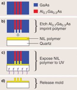
Because it is based on mechanical replication, NIL can achieve lithographic resolutions beyond the limitations set by light diffractions or beam scatterings in conventional lithographic techniques (the pattern-transfer fidelity of NIL is less than 1 nm over the entire wafer) while promising high-throughput patterning. And although NIL is not an optical technique per se, it does incorporate some optical elements, including ultraviolet light sources (for curing) and lasers for alignment of the layers. In addition, the same techniques used to create photolithography masks are used to make the NIL templates.
“The concept of imprint has been around for centuries, if you think of the Chinese wax seal process to authenticate documents,” said Mark Melliar-Smith, president and CEO of Molecular Imprints (Austin, TX), one of the leading providers of step-and-flash UV (versus thermal) imprint lithography tools. “The challenge with thermal imprinting is twofold: heating things up and cooling them down makes it too slow to be commercially viable, and the concept of having heat does not allow very accurate overlay of one pattern on top of another because of thermal expansion.”
In the mid 1990s, Grant Willson of the University of Texas came up with the idea of replacing the wax traditionally used in imprint lithography with a liquid that could then be fixed or hardened with a flash of UV light. He realized that, due to capillary forces, very low viscosity liquids will fill tiny cavities, and he envisioned using a quartz template, created by etching fine patterns into quartz, and a low-viscosity liquid to fill the cavities etched into the surface. When these materials are exposed to UV light, they turn into polymers and intricate patterns can be formed.
“This process happens very quickly and can be done at room temperature, so you can lay one pattern down on top of another,” Melliar-Smith said. “So in the semiconductor industry we can now use this in CMOS manufacturing, where the overlay of one pattern on top of another is crucial.”
The cons
Still, NIL is not without limitations, especially when it comes to chip manufacturing. Foremost among these are the inherent defect issues arising from the very characteristic that enables NIL to fabricate such high-resolution features: the contact between the wafer and the template. Defects are also an issue in the templates used in NIL to achieve single-digit-nanometer resolution. Although fabricated in much the same way as photomasks, these templates cannot be properly inspected with available mask tools, necessitating the use of 1X wafer-inspection tools as an interim solution. The result is manufacturing write-times that can stretch into days for each substrate, making throughput yet another issue.
“Because of its mechanical printing nature, NIL is capable of molecular-level resolution, and as long as you can make a mold or master, you can always replicate it,” said Jim Wang, chief technology officer at NanoOpto (Somerset, NJ), a start-up company founded by Chou. “In addition, because you have the resolution and the concept is so simple, the system is relatively low cost compared to EUV. The downside of NIL is its mechanical nature. When your substrate is not absolutely clean you can get defects such as particle fray. And if your master is not clean, at 50 nm defects can have a huge impact.”
As a result, the semiconductor industry has so far favored the “newer” optical techniques such as EUV and immersion for sub-32 nm lithography—the next node on the International Technology Roadmap for Semiconductors.3 But the industry does appear to be paying more attention to NIL these days; at the SPIE Advanced Lithography meeting (San Jose, CA) earlier this year, for example, there were several discussions about the pros and cons of NIL versus EUV.4 Even Sematech, which has put much more effort into optical lithography, has some projects under way that will impact NIL development; researchers at its Albany, NY, facility, are working to improve EUV mask cleaning and inspection, which should in turn lead to advances in imprint lithography template development, according to Michael Lercel, director of lithography at Sematech (Austin, TX).
“The good thing with NIL is that everything prints, and the bad thing with NIL is that everything prints,” he said. “Nanoimprint is a neat technology with the fundamental advantage of being able to print very small features. But you have to line it up with the semiconductor industry’s requirements in terms of throughput, productivity, and defect inspections for manufacturing ICs. Any technology that is trying to match up with optical lithography in this regard has some serious challenges ahead of it.”
Applications, near and far
As a result, NIL has so far gained more traction in industries that have slightly less-stringent defect, alignment, and throughput requirements than chip manufacturing. In addition to potential markets in sub-32 nm CMOS and post-CMOS devices, NIL is being used in the manufacture of high-brightness LEDs, storage media, MEMS, flat-panel displays, flexible electronics, and biomedical devices. At the Center for Applied NanoBioscience at Arizona State University (Tempe, AZ), for example, researchers have been using NIL for patterning and printing onto polymeric materials to create and manipulate 3-D microenvironments that can provide new ways of manipulating and controlling biomolecules. By spatially mediating the chemical composition and physical properties of a contained environment, they have found they can control biochemical reactions and possibly reduce the complexity of molecular interactions, which could lead to a simplified protocol for preparing biomolecules (or biomarkers) to be used in a diagnostic assay.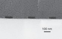
“Our center is interested in developing new processing methods for patterning and printing nanocomposite and polymer materials for a broad range of applications, including organic electronics, molecular diagnostics for early detection of infectious diseases, forensics, and 3-D cell culture systems for studying tumor microenvironments,” said Frederic Zenhausern, director of the Arizona center.
Molecular Imprints, meanwhile, is pursuing applications in the disk-drive markets (such as bit-patterned media) and high-brightness LEDs, while NanoOpto sees its strongest near-term potential in the manufacture of optoelectronic components such as diffractive optics.
But this doesn’t mean that NIL has no future in CMOS manufacturing. In fact, several imprint-enabled production lines are already serving some optics and photonic-crystal markets, and unit-process development and device-prototyping tools are being used by flash-memory and other advanced-CMOS manufacturers. Molecular Imprints has already shipped one of its NIL systems to Toshiba, which is reportedly using it for fabricating NAND flash devices. In addition, in March 2007 Nanonex (Princeton, NJ) delivered its NX-B100 10 nm nanoimprint tool to Los Alamos National Laboratories (Los Alamos, NM). And rival Obducat (Malmö, Sweden) recently introduced an NIL system the company says is capable of imprinting 30 200 mm wafers per hour.
“Defects are a significant issue in CMOS lithography, but I’m certainly not going to throw up my hands and say that imprint [lithography] has too many defect or throughput issues to not be viable in CMOS,” Melliar-Smith said. “However, if you look at the progress EUV has made in defect reduction and what we have done with our imprint tools, they overlap. Both have issues and both have work to be done.”
REFERENCES
1. J. Wang, invited paper, SPIE Advanced Lithography meeting (March 2007).
2. S.Y. Chou, et al., J. Vac. Sci.Technol. B14 (6), (Nov/Dec 1996).
3. www.itrs.net
4. T. Cheyney, SmallTimes (March 8, 2007).
About the Author
Kathy Kincade
Contributing Editor
Kathy Kincade is the founding editor of BioOptics World and a veteran reporter on optical technologies for biomedicine. She also served as the editor-in-chief of DrBicuspid.com, a web portal for dental professionals.