PHOTONICS WEST PREVIEW: Biophotonics leads growth for a February 2013 SPIE Photonics West
“We’re expecting around 1,200 exhibiting companies at SPIE Photonics West again this year [1,214 in 2012], and more than 200 at the BiOS Expo [217 in 2012],” says Marilyn Gorsuch, SPIE Photonics West event manager. “The halls are filling fast, and late-booking companies who want to be a part of the Photonics West Exhibition will be facing the prospect of a waiting list.” Clearly, SPIE Photonics West 2013 continues to be the most popular and well-attended photonics trade show in the United States.
Gorsuch says that technical presentations are currently at 4,454, which is up approximately 5% over last year, and SPIE expects that number to grow as well as the event nears. What is driving the growth? “There are several new conferences in the BiOS program, and the MOEMS-MEMS Symposium has seen a jump in submissions, driven by the areas of microfluidics, bioMEMS, and medical microsystems,” adds Gorsuch. “Clearly, these additions reflect important advances in personalized medicine. Due to the stature of the BiOS Symposium, attendees can expect once again to hear the very latest work in the conference rooms as well as in the always well-attended BiOS Hot Topics event on the opening day.”
SPIE Photonics West 2013 will be held in the Moscone Convention Center in San Francisco, CA from February 2–7, a week later than its typical end-of-January dates. “The shift into February was dictated by existing schedule commitments at Moscone,” says Gorsuch. “We are still somewhat newcomers in this first-tier city, and the convention center has bookings with many other organizations that are five or even ten years out. For the future, we are working with Moscone to keep the event on or as close as possible to the last week in January.”
Once again this year, SPIE Photonics West features the BiOS, LASE, MOEMS-MEMS, OPTO, and the virtual Green Photonics Symposia. And don’t forget the job fair, which will be held February 5–6 from 10 am to 5 pm in the South Hall. From what we’ve seen on LinkedIn, job prospects in photonics have dramatically increased over the past year.
BiOS
It’s looking as though once again, the Biomedical Optics Symposium (BiOS) will represent nearly half of SPIE Photonics West. As of mid-November 2012, “BiOS papers account for 44% of the total papers scheduled at SPIE Photonics West 2013,” according to Gorsuch.
BiOS, the world’s largest biomedical optics and biophotonics symposium and exhibition, will launch SPIE Photonics West when it opens on February 2. The expo will be open both Saturday and Sunday, February 2–3, and the symposium—featuring nearly 2,000 presentations on clinical, translational, and fundamental research and development—will run through the entire week. Forty-three conferences are organized into five major tracks, including the Clinical Technologies and Systems track that will feature an array of work in cancer detection and treatment, with an invited talk on predicting breast cancer response to therapy by Quing Zhu of the University of Connecticut and Liqun Wang of the University of Manitoba (Canada).
Among the new conferences this year are Terahertz and Ultrashort Electromagnetic Pulses for Biomedical Applications, which includes numerous keynote and invited talks, and Optical Methods in Developmental Biology. The new Bioinspired, Biointegrated, Bioengineered Photonic Devices conference will begin with a keynote by John A. Rogers of the University of Illinois at Urbana-Champaign talking about digital cameras in bio-inspired designs.
Another new conference, this one on optogenetics and hybrid-optical control of cells, will begin Saturday and Sunday with keynote addresses by Karl Deisseroth of Stanford University and Ernst Bamberg of Max-Planck-Institut für Biophysik (Germany), respectively. Deisseroth will review development and application of optogenetics, while Bamberg will discuss light-gated ion channels and pumps as optogenetic tools in neuro- and cell biology; both gentlemen have been recognized by numerous organizations for their contributions to the field. Bamberg will also present on this topic at the Saturday evening BiOS Hot Topics plenary event.
As in past years, the two BiOS symposium co-chairs—optical coherence tomography (OCT) pioneer James Fujimoto of the Massachusetts Institute of Technology (MIT) and R. Rox Anderson of the Massachusetts General Hospital and Harvard School of Medicine—will announce the winner of the second annual Britton Chance Award. Then, Sergio Fantini of Tufts University will cue Bamberg and the rest of the speakers: Ben Potsaid of MIT on technology to enable ultrahigh-speed OCT; Dan Oron of Israel’s Weizmann Institute on patterned multiphoton photoactivation in scattering tissue; and Jonathan Sorger of Intuitive Surgical, Inc. on clinical requirements for optical imaging in medical robotics. In addition, Bernard Choi of the Beckman Laser Institute will speak on camera-based functional imaging of tissue hemodynamics; and Mathias Fink of Institute ESPCI in France will discuss a multiwave approach to elasticity imaging for cancer detection. Joe Culver of Washington University in St. Louis is sure to fascinate the audience with his talk on functional optical imaging of the brain, while Vladimir Zharov of the University of Arkansas for Medical Sciences will update the audience on photoacoustic flow cytometry of circulating blood.
A special Sunday afternoon program for academics and entrepreneurs on FDA policies and procedures will feature Yun-Fu Hu of the FDA’s Office of In Vitro Diagnostic Device Evaluation and Safety talking about regulation of in vitro diagnostics.
Finally, SPIE will present for the first time the Biophotonics Technology Innovator Award, which it plans to issue annually to recognize achievements showing strong promise for great impact.
LASE
At the heart of SPIE Photonics West is the topic of light sources and their uses; presentation topics in 2013 for the LASE Symposium include laser source engineering, nonlinear optics, semiconductor lasers and LEDs, laser micro- and nanoengineering, and laser applications.
The many new directions in solid-state laser technology are evident from papers given on solid-state, fiber, and semiconductor lasers. Invited paper 8599-5 from researchers at the University of Hamburg (Germany) details advances in visible and near-infrared (near-IR) femtosecond-laser-written waveguide lasers; both IR and visible devices can be written in clad oxide or fluoride hosts, emitting at 2 W or more. In paper 8599-18, a group from Sotera Defense Solutions (Herndon, VA) and the U.S. Naval Research Lab describes the use of highly transparent doped sesquioxide ceramic for eye-safe solid-state laser materials, which reach efficiencies of up to 74%.
Invited paper 8601-1 on progress in kilowatt-class narrow-linewidth fiber lasers and amplifiers, presented by Imtiaz Majid of Nufern (East Granby, CT), delves into the optimization and packaging of these devices, which can be combined to reach power levels of 100 kW or more. A new fiber-laser geometry based on a ribbon shape is presented by scientists from Lawrence Livermore National Lab (Livermore, CA); such a ribbon could lead to a single-mode laser reaching powers far beyond the theoretical limits of conventional fiber lasers.
Leading-edge in-plane semiconductor lasers are well-represented; for example, a group from the National Institute of Advanced Industrial Science and Technology (Japan) and Hitachi (Japan) describes green and yellow laser diodes based on BeZnCdSe quantum wells (paper 8640-14), which achieve room-temperature continuous-wave outputs of more than 50 mW at the very useful wavelength of 536 nm. Researchers from Osram Opto Semiconductors (Germany) describe progress in high-power blue and green laser diodes and applications (invited paper 8640-15); technologies include direct green lasers emitting up to 200 mW and green phosphor-conversion systems reaching luminance above the level of green LEDs.
Invited paper 8625-40, by Alexis Kavokine of the University of Montpellier 2 (France), covers a new terahertz-emitting vertical-cavity surface-emitting laser (VCSEL) based on gallium nitride (GaN) in which mixed light-matter quasiparticles (exciton-polaritons) stimulate terahertz optical transitions; the lasers are pumped by commercial red LEDs. In paper 8625-46, Seong-Ju Park of Gwangju Institute of Science and Technology (South Korea) describes surface-plasmon-enhanced high-efficiency LEDs that could lead to higher internal quantum efficiencies than produced by today’s devices.
Paper 8600-35, to be presented by researchers from Friedrich-Schiller-University Jena (Germany) and the Council for Scientific and Industrial Research (South Africa), has the intriguing title “Free space propagation without free space.” The group presents a fast technique for measuring the beam-quality factor M2of laser beams in which a spatial light modulator (SLM) is used to digitally simulate the beam’s free-space propagation of the beam, with the result that only one axial beam-measurement position is required.
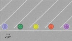
In invited paper 8600-53 on resonance-based CMOS-compatible reconfigurable nanophotonic structures in hybrid material platforms, Ali Adibi of the Georgia Institute of Technology (Atlanta, GA) outlines recent achievements in the development of hybrid multilayer CMOS-compatible lasers resonators and other high-performance reconfigurable photonic devices based on high-Q resonators; for example, an array of miniaturized microdonut optical resonators used for on-chip spectroscopy (see Fig. 1). Paper 8637-8, presented by Cheng-Wei Qiu of the National University of Singapore, delves into the fundamental physics and origin of “pulling” light, describing the workings of photonic tractor beams, and light escalators; he also presents, for the first time, a critical point and how it will help resolve the controversy around these pushing/pulling forces.
And don’t miss the LASE plenary session; there, Martin Wegener of the Karlsruhe Institute of Technology (Germany) describes 3D laser-writing of optical metamaterials that include the first 3D visible-frequency polarization-independent invisibility cloak and the first visible-frequency 3D complete-photonic-band-gap material. The approach relies on stimulated-emission-depletion (STED) to achieve beyond-diffraction-limited dimensions.
MOEMS-MEMS
Microoptoelectromechanical systems (MOEMS) and microelectromechanical systems (MEMS) are the focus of this conference, which includes microfluidics, adaptive optics, and many other micro- and nanostructures under its umbrella.
An invited paper (8609-18) by Andreas Ostendorf of Ruhr-University Bochum (Germany) give a 10-year perspective on the laser generation of sub-100-nm structures; such dimensions, well below the diffraction limit of most optical systems, can be achieved by photonic techniques that range from threshold-dominated multiphoton processes to field enhancement of plasmonic components. Ostendorf also extrapolates these technologies 10 years into the future.
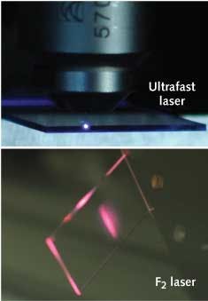
Researchers from the University of Toronto (Canada) present paper 8607-17 on the spectroscopic study of fused-silica glass based on femtosecond near-IR and nanosecond deep-ultraviolet (DUV) laser interactions. Real-time photoluminescence induced by the two types of laser light, together with fluorescence studies, reveal differing reaction pathways that each dominate in the generation of different optical defects that lead to compaction stresses and refractive-index modifications (see Fig. 2).In paper 8616-2, scientists from Femto-ST (France) and the Fraunhofer-Institut für Elektronische Nanosysteme (Germany) describe the use of multi-wafer bonding technology to fabricate a 3D micro-optical lens scanner that can be used in on-chip confocal microscopes and other scanning imaging microsystems; integrated into the device are glass lids, silicon electrostatic x-y and z microactuators, glass microlenses, and ceramic spacers, while through-wafer vias supply the electrical connections. Details of a fully programmable MEMS diffraction grating are presented by a group of French, Swiss, and American researcher in paper 8616-18; an array of 64 slender silicon micromirrors can be electrostatically adjusted in position to spectrally tailor the input of spectroscopic devices.
The stationary-wave integrated Fourier-transform spectrometer (SWIFTS) is the topic of paper 8616-20, given by a group of French researchers, including some at Resolution Spectra Systems, which is commercializing the instrument. Residing on a chip a few millimeters in size, SWIFT is a highly integrated high-resolution spectroscopy technology. Systems based on this technology can typically achieve high spectral resolution with a high signal-to-noise ratio (SNR) over a bandwidth of from several to a few hundred nanometers. The researchers discuss assembly, calibration, and results in the areas of laser analysis, laser spectroscopy, and OCT.
Image transmission through an opaque material is discussed in invited paper 8617-11 by a team from Institut Langevin (France). The researchers’ topic and results are an example of the emerging technology of imaging through turbid and scattering media. Here, the researchers describe how they can measure the complicated mesoscopic optical transmission channels that allow light to traverse through an “opaque” (highly scattering) medium, producing a transmission matrix that allows the recovery of a high-fidelity image even for highly complex propagation paths.
OPTO
“Having the honor of chairing the 2013 OPTO Symposium at Photonics West, I am delighted to see its remarkable growth in size and impact continuing unabated,” says David L. Andrews, professor of chemical physics at the University of East Anglia (Norwich, England). “SPIE is particularly good at cultivating and supporting a fervent mix of science and technology, and this is a real showcase event. Conferences in seven separate tracks will be covering all of the latest developments in optical materials and devices, as well as research innovations where the interplay of experiment with theory and simulation is particularly rich.” Andrews adds, “Amongst numerous other developments, some of the most eagerly anticipated news will be on the latest advances in quantum applications, with plenary and other invited talks focusing on quantum memories, quantum optomechanics, and quantum optical vortices.”
“Photonics West’s astounding growth reflects the resilience of photonics science and technology in times of economic uncertainty,” says Alexei Glebov, OPTO Symposium co-chair and CEO and president of OptiGrate (Orlando, FL). “With more than 1,500 papers, OPTO will showcase the latest photonics trends such as quantum optics in a variety of applications, nanophotonics, silicon photonics, and engineered nanostructures for optical interconnects, lab-on-a-chip, photovoltaics, sensing, as well as green photonic technology advances in photovoltaic, energy efficient communication, and energy saving lighting solutions.”
Glebov recommends the following papers that may be of high interest: Quantum Optomechanics plenary paper 8637-1 from Markus Aspelmeyer of the University of Vienna (Austria); Towards a Comprehensive Silicon-Photonic Platform, invited paper 8628-3 from Michael Watts of MIT; Theory-Guided Nano-Engineering of Organic Electro-Optic Materials for Hybrid Silicon Photonic, Plasmonic, and Metamaterial Devices, a keynote presentation (paper 8622-19) from Larry R. Dalton at the University of Washington; Group IV Photonics for the Mid Infrared plenary paper 8629-1 from Richard Soref of the University of Massachusetts (Boston); and 2D-Photonic Crystals for Record Solar Cell Efficiency, invited paper 8632-13 from Eli Yablonovitch and colleagues at the University of California, Berkeley.
Green Photonics
In addition to the panel discussion on Emerging Growth Opportunities in Sustainable Technology moderated by Steve Eglash, executive director of the Energy and Environment Affiliates Program at Stanford University, the Green Photonics Symposium offers more than 65 papers on green photonics research organized around four topical areas: Solid State Lighting and Displays; Laser-assisted Manufacturing and Micro/Nano Fabrication; Communications; and Renewable Energy Generation and Photovoltaics.
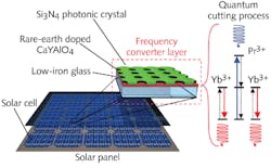
SPIE recommends the following “hot papers” in the Green Photonics Symposium: Light Quality and Efficiency of Consumer Grade Solid State Lighting Products, paper 8641-44 from Carsten Dam-Hansen and colleagues at the Technical University of Denmark that reveals the results of a two-year study comparing solid-state lighting to incandescent and halogen lamps, exploring lumen output and color maintenance for 8,000 hours of data; and Rare-Earth Doped Planar 2D-Photonic Crystals for Quantum Cutting in Solar Cells, paper 8620-15, presented by Thierry Deschamps and a host of fellow researchers from the CNRS and the University of Lyon (France), which discusses a new concept that combines a thin rare-earth-doped layer with a photonic crystal layer to allow efficient conversion from UV-blue photons to near-IR photons with a quantum yield higher than 1—a process defined as quantum cutting (see Fig. 3).Other special events
There are always great refreshments (and networking opportunities) at the SPIE Photonics West conference reception, to be held Monday, February 4 from 7-8:30 pm. Not to mention the Speed Networking Social, and Women in Optics Panel and Roundtable; must-see events to put on your social calendar.
And each year, Laser Focus World staff members attend the Industry Events to hear prestigious panel members discuss Silicon Photonics and Photonic Integrated Circuits (Tuesday, February 5, 2-3 pm), Emerging Growth Opportunities in Sustainable Technologies (Tuesday, February 5, 3:30-4:30 pm), and the always popular (get there early for seating) Executive Perspectives on the World of Optics and Photonics (Wednesday, February 6, 2-3 pm). Other Industry Events include the potential to win $10,000 in the SPIE Startup Challenge (see http://spie.org/x88933.xml) on Wednesday, February 6, 3:30-6 pm, and don’t miss the Government Initiatives and Opportunities for Growth in Photonics from SPIE executive director Eugene Arthurs on Thursday, February 7 from 8:45-9:15 am.
Now in its 25th year and always held in conjunction with SPIE Photonics West, the 2013 Lasers & Photonics Marketplace Seminar will be held Monday, February 4 at the W Hotel in San Francisco (just a block or so from Moscone). Laser Focus World and Strategies Unlimited invite you to the only comprehensive qualitative and quantitative laser market seminar in the industry, with a keynote presentation this year from Valentin Gapontsev of IPG Photonics and several other important presentations from prominent industry leaders on a variety of laser and photonic topics.
And when the overwhelming amount of technology content is just too much to bear, all exhibitors should take time to eat, drink, and relax at PennWell’s annual Billiards Night at Jillian's Billiards Club, just around the corner from Moscone at 101 4th St., Tuesday, February 5 from 5:30–7:30 pm. Drinks (well, two tickets each) are on us!
About the Author

Gail Overton
Senior Editor (2004-2020)
Gail has more than 30 years of engineering, marketing, product management, and editorial experience in the photonics and optical communications industry. Before joining the staff at Laser Focus World in 2004, she held many product management and product marketing roles in the fiber-optics industry, most notably at Hughes (El Segundo, CA), GTE Labs (Waltham, MA), Corning (Corning, NY), Photon Kinetics (Beaverton, OR), and Newport Corporation (Irvine, CA). During her marketing career, Gail published articles in WDM Solutions and Sensors magazine and traveled internationally to conduct product and sales training. Gail received her BS degree in physics, with an emphasis in optics, from San Diego State University in San Diego, CA in May 1986.
John Wallace
Senior Technical Editor (1998-2022)
John Wallace was with Laser Focus World for nearly 25 years, retiring in late June 2022. He obtained a bachelor's degree in mechanical engineering and physics at Rutgers University and a master's in optical engineering at the University of Rochester. Before becoming an editor, John worked as an engineer at RCA, Exxon, Eastman Kodak, and GCA Corporation.

Barbara Gefvert
Editor-in-Chief, BioOptics World (2008-2020)
Barbara G. Gefvert has been a science and technology editor and writer since 1987, and served as editor in chief on multiple publications, including Sensors magazine for nearly a decade.
