Graphene brings transparency and flexibility to solar cells
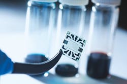
A new flexible, transparent solar cell developed at the Massachusetts Institute of Technology (MIT; Cambridge, MA) is bringing a future closer wherein solar cells are all around us--on windows and walls, cell phones, and laptops. The device combines low-cost organic (carbon-containing) materials with electrodes of graphene, a flexible, transparent material made from inexpensive and abundant carbon sources.
RELATED ARTICLE: Researchers detail transparent graphene sensor technology for bioimaging, optogenetics
This advance in solar technology was enabled by a novel method of depositing a one-atom-thick layer of graphene onto the solar cell--without damaging nearby sensitive organic materials. Until now, developers of transparent solar cells have typically relied on expensive, brittle electrodes that tend to crack when the device is flexed. The ability to use graphene instead is making possible truly flexible, low-cost, transparent solar cells that can turn virtually any surface into a source of electric power.
Photovoltaic solar cells made of organic compounds would offer a variety of advantages over today's inorganic silicon solar cells. They would be cheaper and easier to manufacture. They would be lightweight and flexible rather than heavy, rigid, and fragile, and so would be easier to transport, including to remote regions with no central power grid. And they could be transparent. Many organic materials absorb the ultraviolet and infrared components of sunlight but transmit the visible part that our eyes can detect. Organic solar cells could therefore be mounted on surfaces all around us and harvest energy without our noticing them.
Two key problems have slowed the wholesale adoption of graphene electrodes. The first problem is depositing the graphene electrodes onto the solar cell. Most solar cells are built on substrates such as glass or plastic. The bottom graphene electrode is deposited directly on that substrate--a task that can be achieved by processes involving water, solvents, and heat. The other layers are then added, ending with the top graphene electrode. But putting that top electrode onto the surface of the so-called hole transport layer (HTL) is tricky.
"The HTL dissolves in water, and the organic materials just below it are sensitive to pretty much anything, including water, solvents, and heat," says EECS graduate student Yi Song, a 2016-2017 Eni-MIT Energy Fellow and a member of Kong's Nanomaterials and Electronics Group. As a result, researchers have typically persisted in using an ITO electrode on the top.
The second problem with using graphene is that the two electrodes need to play different roles. The ease with which a given material lets go of electrons is a set property called its work function. But in the solar cell, just one of the electrodes should let electrons flow out easily. As a result, having both electrodes made out of graphene would require changing the work function of one of them so the electrons would know which way to go--and changing the work function of any material is not straightforward.
For the past three years, Kong and Song have been working to solve these problems. They first developed and optimized a process for laying down the bottom electrode on their substrate. In that process, they grow a sheet of graphene on copper foil. They then transfer it onto the substrate using a technique demonstrated by Kong and her colleagues in 2008. Initially, the electrodes that Song and Kong fabricated using this process didn’t perform well. Song decided that adding glue to the stamp might be the way to go--but as a layer on top of the graphene.
The process not only improved performance but also brought an unexpected side benefit. The researchers thought their next task would be to find a way to change the work function of the top graphene electrode so it would differ from that of the bottom one, ensuring smooth electron flow. But that step wasn’t necessary. Their technique for laying down the graphene on the HTL actually changes the work function of the electrode to exactly what they need it to be.
The power conversion efficiencies (PCEs) for all their graphene/graphene devices ranged from 2.8 to 4.1%. While those values are well below the PCEs of existing commercial solar panels, they’re a significant improvement over PCEs achieved in prior work involving semitransparent devices with all-graphene electrodes, the researchers say.
Measurements of the transparency of their graphene/graphene devices yielded further encouraging results. The all-graphene devices showed optical transmittance of 61% across the whole visible regime and up to 69% at 550 nm. Those values [for transmittance] are among the highest for transparent solar cells with comparable power conversion efficiencies in the literature.
The researchers note that their organic solar cell can be deposited on any kind of surface, rigid or flexible, transparent or not. "If you want to put it on the surface of your car, for instance, it won't look bad," says Kong. "You'll be able to see through to what was originally there." The ability to deposit the solar cell on any surface makes it promising for use on consumer electronics.
The researchers are now working to improve the efficiency of their graphene-based organic solar cells without sacrificing transparency. According to their calculations, the maximum theoretical PCE achievable at their current level of transparency is 10%. "Our best PCE is about 4 percent, so we still have some way to go," says Song.
SOURCE: MIT; http://news.mit.edu/2017/mit-researchers-develop-graphene-based-transparent-flexible-solar-cells-0728
About the Author

Gail Overton
Senior Editor (2004-2020)
Gail has more than 30 years of engineering, marketing, product management, and editorial experience in the photonics and optical communications industry. Before joining the staff at Laser Focus World in 2004, she held many product management and product marketing roles in the fiber-optics industry, most notably at Hughes (El Segundo, CA), GTE Labs (Waltham, MA), Corning (Corning, NY), Photon Kinetics (Beaverton, OR), and Newport Corporation (Irvine, CA). During her marketing career, Gail published articles in WDM Solutions and Sensors magazine and traveled internationally to conduct product and sales training. Gail received her BS degree in physics, with an emphasis in optics, from San Diego State University in San Diego, CA in May 1986.