Interferometric lithography creates 3D graphene electrodes
Knowing that it would be advantageous to have an electrode that is similar in size to the diffusion distance of molecules in a reaction in order to increase the mass transport of reactants, researchers at Sandia National Laboratories are using interferometric lithography to create three-dimensional (3D) graphene materials that can be used to produce a 3D graphene electrode for simultaneous detection of dopamine, uric acid, and ascorbic acid, among other electrochemical applications.
Related Article
The standard carbon electrode (SCE) is a planar glassy electrode based on amorphous carbon arranged in the sp3 configuration, where the atoms form tetrahedra. The SCE is used in many electrochemical applications because of the formation of a chemical boundary layer in reduction and oxidation reactions, leading to diffusion of the reaction products. However, the SCE does not have a large enough surface area to enable high reaction rates in some catalytic processes.
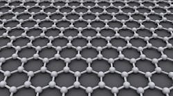
Furthermore, one cannot use sp3-bonded electrodes in some sensing processes that are possible when carbon atoms are arranged in the sp2 configuration, in which the atoms form flat sheets, as in graphene and carbon nanotubes. Ideally, producing an sp2 carbon electrode with a large surface area on a micrometer scale—essentially 3D graphene—expands the range of possible applications.
Several research groups have converted 3D nickel foams that have 3D pores on the hundred-micrometer scale, into 3D graphene by conformally depositing carbon via chemical vapor deposition and annealing the structure. Because the nickel foam is created electrochemically, its geometry is randomly determined with little control over the size and spacing of its pores, which makes it hard to design a graphene electrode on the same scale as the molecular diffusion distance.
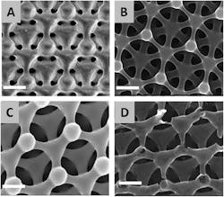
The Sandia researchers overcame this problem using interferometrically defined 3D scaffolds, where the geometry of the scaffold is controlled by varying its exposure to radiation. The specific patterning technique is interferometric lithography, in which coherent plane waves undergo interference in space to generate a 2D fringe pattern. Using an ultraviolet (UV) laser, the fringe pattern can expose a photoresist. Depending on the number of exposures and the rotation between each exposure, the team can produce a 1D, 2D, or 3D photoresist pattern after development.
Furthermore, they can form a face-centered cubic structure by three successive periods of exposure to two beams that are tilted with respect to a line perpendicular to the substrate, with the substrate rotated by 120 degrees between each exposure. After heating the resist pattern, non-carbon species in the resist are volatilized and boil off, while the carbon remains behind. The photoresist pattern shrinks significantly, but the basic morphology remains intact, resulting in a 3D network of sp3-bonded carbon with micrometer-scale pores.
To convert this amorphous carbon scaffold into sp2-bonded carbon, the team forms a conformal coating of nickel on the scaffold by sputtering. After annealing, carbon diffuses through the nickel coating and, surprisingly, nickel and carbon completely switch places, forming a hollow 3D nickel–carbon scaffold that is confirmed to be an sp2-bonded carbon via x-ray spectroscopy and micro-Raman scans.
The proven potential of 3D graphene electrodes to increase reaction rates and mass transport in electrochemical reactions can be further enhanced both before and after pyrolytic treatment. In further research, the electrode surface area is dramatically increased by incorporating nanoscale pores in the existing micrometer-scale porous structure using sacrificial nanoparticles in the resist stage. The team says they can also potentially produce multifunctional scaffolds by heterogeneously decorating scaffolds with functional nanoparticles.
SOURCE: SPIE Online Newsroom; http://spie.org/x114751.xml?highlight=x2400&WT.mc_id=KNRNANOE
About the Author

Gail Overton
Senior Editor (2004-2020)
Gail has more than 30 years of engineering, marketing, product management, and editorial experience in the photonics and optical communications industry. Before joining the staff at Laser Focus World in 2004, she held many product management and product marketing roles in the fiber-optics industry, most notably at Hughes (El Segundo, CA), GTE Labs (Waltham, MA), Corning (Corning, NY), Photon Kinetics (Beaverton, OR), and Newport Corporation (Irvine, CA). During her marketing career, Gail published articles in WDM Solutions and Sensors magazine and traveled internationally to conduct product and sales training. Gail received her BS degree in physics, with an emphasis in optics, from San Diego State University in San Diego, CA in May 1986.

