SEMICONDUCTOR LASERS: Two-color ‘nanosheet’ lasers light the way for displays and illumination
The quest for laser-based broadband emitters for lighting and other applications has received a boost, with researchers at Arizona State University (ASU; Tempe, AZ) unveiling a single, nanoengineered heterostructure that lases at 526 and 623 nm.
Solid-state structures that emit across the visible spectrum will surely lead to applications in commercial lighting and displays. Cracking the problem in semiconductor structures would also advance applications such as multispectral detection and high-efficiency photovoltaics.
The problem with semiconductors has traditionally been limitations imposed by their crystalline structure, with semiconductor lasers emitting in narrow wavelength ranges. Recent work has focused on achieving more broadband emission simply by engineering chemically different structures with differing bandgaps that allow them to emit at different wavelengths.
It is a pursuit that creates a great deal of stress—specifically, the stresses at the interfaces between different semiconductor materials. This “lattice mismatch” strains the semiconductor crystal structure and adversely affects output. Engineering optical cavities to support the different colors is also tricky. But help may be at hand in the form of nanostructures such as nanowires, nanobelts, and nanosheets.
Much recent work has attempted to achieve multicolor lasing from nanowires. In 2008, Cun-Zheng Ning and his team at Arizona State University (Tempe, AZ) demonstrated nanowires based on cadmium sulfur selenide (CdSSe), varying the optical properties of nanowires grown with chemical-vapor deposition (CVD) by tightly controlling the local substrate temperature during growth. The resulting structures emitted between about 500 and 700 nm.1 In 2010, they advanced the technique to produce emission across the entire visible spectrum, growing nanowires under conditions of varying both temperature and chemical reagent, and creating CdSe and zinc sulfide (ZnS) nanowires with bandgaps at about 350 and 710 nm.2
“In those papers, we were able to achieve lasing or emission in a wide spectral range on a single growth substrate but over many wires,” says Ning.
Then in 2011, a group, including regular collaborators with the ASU team, showed single-nanowire, full-visible-range operation using similar gradient-based growth techniques.3 “Lasing from such a single nanowire is very challenging,” says Ning. “The main challenge is to design different cavities for different colors—we have tried to use similar wires to achieve lasing, and it did not work.”
That is particularly tricky for heterostructures with multiple-bandgap materials. Shorter wavelengths from the wide-bandgap materials will tend to be absorbed in the narrow-gap parts so that only the longer-wavelength light can reach threshold and lase, Ning explains. “This is why we finally—after many experiments—came to a nanosheet, where two parallel cavities can be created for two colors.”
Nanosheet elements
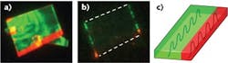
Ning’s team expanded on the vapor-liquid-solid CVD technique shown off in the prior work, using CdS and CdSe powder starting materials and a silicon substrate with a thin gold film as catalyst. The growth cycles were tuned to build CdS layers first, leading to a wide central CdS-dominated region surrounded by CdSe edges. This wide central region provides optical confinement for the short-wavelength emission. These “nanosheet” elements form two rectangular, coupled cavities side by side—a configuration that is clear under continuous-wave 405 nm laser illumination (see figure).
“We tried various approaches, and many of them failed. This side-by-side structure worked really well,” notes Ning.
Nanosheets were cleaved from the larger substrate, mounted onto a sapphire substrate, and optically pumped with a frequency-tripled Nd:YAG laser emitting at 355 nm, resulting in distinct lasing at 534 and 592 nm.
When the researchers adjusted their recipe for growing the films—by completely cutting off supply of CdS to the furnace when initiating the CdSe growth—the separation between the two lasing modes was greater: 526 and 623 nm.4 These results are the first observation of simultaneous lasing in two colors on a single, monolithic semiconductor structure.
What’s more, the technique hints at more progress in this direction; finely tuned heterostructure growth techniques could lead to many more than two colors. “There is no essential limit in principle,” Ning says, though he concedes that “there are some practical or technological challenges one has to overcome.”
The finer details of nanosheet growth and lattice-matching in these different materials is still an inexact experimental science. And for real applications—in particular, for lighting and displays—the next clear step is electrical injection rather than laser illumination. But the approach seems to allow greater flexibility in design and eventual manufacture than many other options in the long-running search for a compact and simple multicolor source.
REFERENCES
1. A. Pan et al., Nano Lett., doi:10.1021/nl803456k (2008).
2. A. Pan et al., ACS Nano, doi:10.1021/nn901699h (2010).
3. Z. Yang et al., ACS Nano, doi:10.1021/nl203529h (2011).
4. F. Fan et al., Semicond. Sci. Tech., doi:10.1088/0268-1242/28/6/065005 (2013).