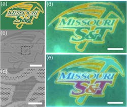
A color printing process from researchers at Missouri University of Science and Technology (Missouri S&T; Rolla, MO) is giving new meaning to the term "read the fine print." The nanoscale print features are very fine—visible only with the aid of a high-powered electron microscope.
RELATED ARTICLE: Silicon films on metal create perfectly absorbing optical color filters
The researchers describe their "no-ink" printing method in the latest issue of the Nature Publishing Group journal Scientific Reports and illustrate their technique by reproducing the Missouri S&T athletic logo on a nanometer-scale surface.
Not unlike color laser marking via diffraction patterns, the method involves the use of thin sandwiches of nanometer-scale metal-dielectric materials known as metamaterials that interact with light in ways not seen in nature. Experimenting with the interplay of white light on sandwich-like structures, or plasmonic interfaces, the researchers developed what they call “a simple but efficient structural color printing platform” at the nanometer-scale level. They believe the process holds promise for future applications, including nanoscale visual arts, security marking and information storage.
The researchers' printing surface consists of a sandwich-like structure made up of two thin films of silver separated by a "spacer" film of silica. The top layer of silver film is 25 nm thick and is punctured with tiny holes created by a microfabrication process known as focused ion beam milling. The bottom layer of silver is four times thicker than the top layer but still minuscule at 100 nm. Between the top and bottom films lies a 45 nm thick silica dielectric spacer.
The researchers created a scaled-down template of the athletic logo and drilled out tiny perforations on the top layer of the metamaterial structure. Under a scanning electron microscope, the template looks like a needlepoint pattern of the logo. The researchers then beamed light through the holes to create the logo using no ink—only the interaction of the materials and light.
By adjusting the hole size of the top layer, light at the desired frequency was beamed into the material with a perfect absorption. This allowed researchers to create different colors in the reflected light and thereby accurately reproduce the S&T athletic logo with nanoscale color palettes. The researchers further adjusted the holes to alter the logo's official green and gold color scheme to introduce four new colors (an orange ampersand, magenta "S" and "T," cyan pickaxe symbol and navy blue "Missouri").
"To reproduce a colorful artwork with our nanoscale color palettes, we replaced different areas in the original image with different nanostructures with specified hole sizes to represent various visible colors," says Xiaodong Yang, an assistant professor at Missouri S&T, who leads the Nanoscale Optics Laboratory in the university's mechanical and aerospace engineering department. "We chose the athletic logo to fill that need."
"Unlike the printing process of an inkjet or laserjet printer, where mixed color pigments are used, there is no color ink used in our structural printing process—only different hole sizes on a thin metallic layer," says Jie Gao, an assistant professor of mechanical and aerospace engineering at Missouri S&T and a co-author of the paper.
In their paper, the authors note that the process resulted in "pure colors with high brightness" with little need for protective coatings. The researchers believe the process could lead to "high-performance, pigment-free color printing and relevant applications such as security marking and information storage."
SOURCE: Missouri University of Science and Technology; http://news.mst.edu/2015/06/researchers-demonstrate-no-ink-color-printing-with-nanomaterials/
About the Author

Gail Overton
Senior Editor (2004-2020)
Gail has more than 30 years of engineering, marketing, product management, and editorial experience in the photonics and optical communications industry. Before joining the staff at Laser Focus World in 2004, she held many product management and product marketing roles in the fiber-optics industry, most notably at Hughes (El Segundo, CA), GTE Labs (Waltham, MA), Corning (Corning, NY), Photon Kinetics (Beaverton, OR), and Newport Corporation (Irvine, CA). During her marketing career, Gail published articles in WDM Solutions and Sensors magazine and traveled internationally to conduct product and sales training. Gail received her BS degree in physics, with an emphasis in optics, from San Diego State University in San Diego, CA in May 1986.
