INSTRUMENTATION FOR NANOPHOTONICS: Printed photonics require nanoscale measurements
FRANZ PADINGER
The fast-growing field of printed photonics enables rapid development and production of lightweight, ultrathin, bendable photonic devices with nanoscale features. This technology demands high material quality, precise material deposition, and application-specific optical, electrical, chemical, and mechanical properties. A wide variety of instrumentation exists today for precision measurement. But which are best for printed photonics? At Nanoident Technologies, which manufactures printed photodetectors and other devices, we use a combination of high-precision tools to image and measure critical parameters throughout the R&D and production cycles.
Printed photonics
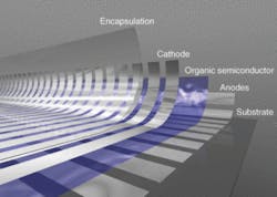
Printing is a relatively new way of producing semiconductor photonic devices. Rather than using the complex, expensive, and time-consuming subtractive processes of traditional semiconductor-device fabrication that relies on solid silicon as a substrate material, printed photonic devices are created with an additive process, using printing techniques such as inkjet or offset to deposit liquid semiconductor materials. These materials consist of several layers or three-dimensional bulks of printable semiconductors, such as photoactive conjugated polymers and/or nanoparticles in solvents. These “inks” are formulated to have application-specific spectral properties, eliminating the need for optical filters. A typical finished device, such as a photodetector, consists of at least one photoactive layer sandwiched between two electrode layers (see Fig. 1), and can include an integrated organic-light-emitting-diode light source, interconnects, or other features.
Several key parameters must be precisely controlled. To begin with, functional materials must have the proper chemical composition as well as precise optical, electrical, and mechanical characteristics. The required properties cannot be compromised during processing, and some properties are actually developed or improved through special processing steps; for instance, curing can be used to “melt” particles together, creating a better electrical connection. It is also important to have smooth, continuous material coverage, accurate feature size, and exact spacing. Typical lateral feature size is on the order of 10 µm, with submicrometer tolerance. This is not nearly as small as traditional semiconductor feature size, but is nevertheless critical to proper device function.
Layer thickness is quite important to device function; layers are on the order of 20 to 200 nm thick, with nanometer tolerances. Each layer also must be relatively smooth to provide a good interface to the next layer. Because of the degree of precision required for printed photonics, nanoscale impurities and defects can have devastating effects on the finished device.
Several imaging and measurement techniques are available to validate material and deposition quality at the nanoscale. Nanoident uses several instruments to characterize and validate material and device properties in its R&D and manufacturing processes.
Optical profiler
An optical profiler is a purely optical system for measuring height and identifying surface features, and can operate in white-light-interferometer or monochromatic mode. Optical profiling is a noncontact, nondestructive technique that can measure through transparent material. It is relatively easy to use and images can be taken in seconds.
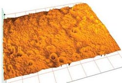
In white-light-interferometer mode, light is split to illuminate both the sample and a reference mirror. The light is then recombined and detected by a CCD camera. The sample is moved vertically through a specified range and an image is taken at each distance. An interference pattern can be seen when the reference mirror and the sample are both the same distance from the splitter. For each pixel, software calculates the height of maximum interference. Because the distance to the reference mirror remains constant, the heights of each pixel can then be calculated. Lateral resolution of this method is approximately 1 µm; absolute height can be measured with single-nanometer accuracy up to several microns, making this a good solution for samples with a varied profile (see Fig. 2).
In monochromatic-light mode, the sample is kept still while the phase of the reference beam is modulated. Software records this “phase image” and transforms it into height information. However, only relative height can be measured, up to one-quarter wavelength (or roughly 100 nm) but with better than 1 nm resolution. This mode is best suited for relatively smooth surfaces without sudden jumps, where greater detail is needed.
We use this instrument primarily to determine the quality of deposited layers in terms of layer thickness and smoothness. It is a good tool to identify surface defects such as pinholes, bubbles, and bumps. It indicates the quality of the deposited layer and the sharpness of the edges.
Atomic-force microscope
Despite its name, the atomic-force microscope (AFM) is primarily a mechanical rather than an optical device, although it does rely on optical technology. The AFM probe is a nanoscale needle mounted on a cantilever. A laser illuminates the cantilever, and as the needle scans the surface of the sample, a photodetector senses light deflection when the cantilever bends.
The AFM can be operated in contact or noncontact (tapping) mode. In contact mode, the instrument tries to keep deflection constant by moving the needle up or down while scanning. The combination of needle movement and deflection are used to calculate the profile of the sample. This technique provides approximately 1 nm resolution in all dimensions. This is considered a destructive method, although careful operation will minimize damage.
In tapping mode, the needle is oscillated close to its resonant frequency just above the surface. As it scans, the instrument tries to keep the amplitude of oscillation constant by moving the needle up or down. By measuring the combination of needle movement and amplitude, a surface profile can be calculated with a resolution of approximately 10 nm. This method is less destructive than the contact mode.
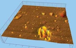
In either mode, a sharper tip provides higher resolution but can cause more damage. The field of view is rather narrow, typically well under one millimeter; maximum material height is only a few microns (see Fig. 3).
We use the AFM primarily for the same purposes as the optical profiler, but when higher resolution is needed. For instance, when a defect is found with the optical profiler, the AFM can be used for closer inspection. Because it can measure at the atomic level, the AFM can indicate how well materials were mixed, and whether the solvents must be adjusted. However, this tool has much wider application. For instance, it is possible to apply voltage to the bottom electrode and place the AFM tip onto the top electrode to measure electrical properties.
Raman spectroscopy
In Raman spectroscopy, the interaction between light and matter is analyzed by measuring molecular vibrations. A laser light source illuminates the sample; light emitted (scattered) from the sample is collected with a lens and detected with a CCD camera. Most of the scattered photons have the same frequency as the incident light, but some are measured at different frequencies. This occurs because the incident light causes changes in the vibration of the molecule. The analysis, plotted as the intensity of scattered light at a range of frequencies, provides a spectral profile of the sample’s chemistry. Each material has a unique spectral fingerprint.
This technique can be used with samples in any form-gas, liquid, powder, or solid. Very small samples can be analyzed-as little as one microliter of liquid or one cubic micrometer of powder. Lateral resolution is roughly 100 nm with a height resolution of approximately 200 nm, which is quite sufficient for chemical characterization.
In one Raman analysis technique, a spectral map of the sample is created that indicates varying intensity of a specific spectral band or spectral range. When compared to a corresponding visual image, this technique can be used to explore visible features and can also detect features not visible by other means. By varying the wavelength of the light source, it enables a “look” inside the sample to determine the morphology of the deposited layers or their interaction.
First and foremost, Raman spectroscopy is used to test the chemical composition or purity of materials; the vast majority of Raman users require only these capabilities. However, because molecular vibration varies with the environment, Raman spectroscopy is also sensitive to a variety of factors, including temperature, sample state, chemical or mechanical impurities, mechanical and electrical strain, electric or magnetic fields, current flow, charge state, and interfaces (interaction with other materials, such as the substrate).
We use this tool in a variety of situations that include investigating small spots on deposited material, verifying the effects of curing processes, determining electrical suitability of materials, analyzing the effects of interfaces, and studying encapsulation effects.
When used by highly skilled operators, Raman spectroscopy is an excellent research tool. However, software can be used to automate a variety of pass/fail tests for high-speed production applications. When used with remote fiber-optic probes, software automation can even enable real-time control of production processes; for instance, monitoring a curing process to prevent overheating.
Combining tools
Each of these tools in isolation can measure different features and detect different problems. However, only when multiple tools are combined is it possible to get a detailed understanding of printed photonic devices and their nanoscale features.
In the lab, these tools can help determine material quality and formulation as well as test prototypes to validate production approaches and aid in process design. They can be used to analyze problems and suggest solutions. In the factory, combined with other tools such as optical scanners and high-speed cameras, they can be used to validate production processes, identify nonconforming product, and provide valuable feedback for continuous improvement. But in either context, the combination of these tools provides what none can do in isolation-a detailed understanding of the nanoscale world of printed photonics.
Tell us what you think about this article. Send an e-mail to [email protected].
FRANZ PADINGER is cofounder and chief technical officer of Nanoident Technologies, Untere Donaulaende 21-25, A-4020 Linz, Austria; e-mail: [email protected]; www.nanoident.com.


