Light-projection chip from Caltech has no moving parts
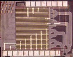
Details of a light-bending or light-projection silicon chip developed by Ali Hajimiri, Thomas G. Myers Professor of Electrical Engineering, and researchers in his laboratory at the California Institute of Technology (Caltech; Pasadena, CA) were presented at the Optical Fiber Communication (OFC) conference in San Francisco on March 10. The silicon chip acts as a lens-free projector or light-steering device without any lenses or mechanical, moving parts, and could one day end up in your cell phone.
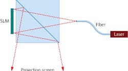
Traditional projectors pass a beam of light through a tiny image, using lenses to map each point of the small picture to corresponding points on a large screen. The Caltech chip eliminates the need for bulky and expensive lenses and bulbs and instead uses a so-called integrated optical phased array (OPA) to project the image electronically with only a single laser diode as light source and no mechanically moving parts.
Hajimiri and his colleagues were able to bypass traditional optics by manipulating the coherence of light—a property that allows the researchers to "bend" the light waves on the surface of the chip without lenses or the use of any mechanical movement. If two waves are coherent in the direction of propagation—meaning that the peaks and troughs of one wave are exactly aligned with those of the second wave—the waves combine, resulting in one wave, a beam with twice the amplitude and four times the energy as the initial wave, moving in the direction of the coherent waves.
"By changing the relative timing of the waves, you can change the direction of the light beam," says Hajimiri. For example, if 10 people kneeling in line by a swimming pool slap the water at the exact same instant, they will make one big wave that travels directly away from them. But if the 10 separate slaps are staggered—each person hitting the water a half a second after the last—there will still be one big, combined wave, but with the wave bending to travel at an angle, he says.
Using a series of pipes for the light called phase shifters, the OPA chip similarly slows down or speeds up the timing of the waves, thus controlling the direction of the light beam. To form an image, electronic data from a computer are converted into multiple electrical currents; by applying stronger or weaker currents to the light within the phase shifter, the number of electrons within each light path changes—which, in turn, changes the timing of the light wave in that path. The timed light waves are then delivered to tiny array elements within a grid on the chip. The light is then projected from each array in the grid, the individual array beams combining coherently in the air to form a single light beam and a spot on the screen.
As the electronic signal rapidly steers the beam left, right, up, and down, the light acts as a very fast pen, drawing an image made of light on the projection surface. Because the direction of the light beam is controlled electronically—not mechanically—it can create a sort of line very quickly. Since the light draws many times per second, the eye sees the process as a single image instead of a moving light beam, says Hajimiri.
"The new thing about our work is really that we can do this on a tiny, one-millimeter-square silicon chip, and the fact that we can do it very rapidly—rapidly enough to form images, since we phase-shift electronically in two dimensions," says Behrooz Abiri, a graduate student in Hajimiri's group and a coauthor on the paper. So far, the images Hajimiri and his team can project with the current version of the chip are somewhat simple—a triangle, a smiley face, or single letters, for example. However, the researchers are currently experimenting with larger chips that include more light-delivering array elements that—like using a larger lens on a camera—can improve the resolution and increase the complexity of the projected images.
In their recent experiments, Hajimiri and his colleagues have used the silicon chip to project images in infrared light, but additional work with different types of semiconductors will also allow the researchers to expand the tiny projector's capabilities into the visible spectrum. "Right now we are using silicon technology, which works better with infrared light. If you want to project visible light, you can take the exact same architecture and do it in what's called compound semiconductor III-V technology," says Firooz Aflatouni, another coauthor on the paper, who in January finished his two-year postdoctoral appointment at Caltech and joined the University of Pennsylvania as an assistant professor. "Silicon is good because it can be easily integrated into electronics, but these other compound semiconductors could be used to do the same thing."
"In the future, this can be incorporated into a phone, and since there is no need for a lens, you can have a phone that acts as a projector all by itself," Hajimiri says. However, although the chip could easily be incorporated into a cell phone, he points out that a tiny projection device can have many applications such as for light detection and ranging or LIDAR. Current LIDAR technology requires complex, bulky, and expensive equipment—equipment that could be streamlined and simplified to a single chip at a much lower cost. Numerous other applications are possible.
SOURCE: Caltech; http://www.caltech.edu/content/bending-light-tiny-chip
About the Author

Gail Overton
Senior Editor (2004-2020)
Gail has more than 30 years of engineering, marketing, product management, and editorial experience in the photonics and optical communications industry. Before joining the staff at Laser Focus World in 2004, she held many product management and product marketing roles in the fiber-optics industry, most notably at Hughes (El Segundo, CA), GTE Labs (Waltham, MA), Corning (Corning, NY), Photon Kinetics (Beaverton, OR), and Newport Corporation (Irvine, CA). During her marketing career, Gail published articles in WDM Solutions and Sensors magazine and traveled internationally to conduct product and sales training. Gail received her BS degree in physics, with an emphasis in optics, from San Diego State University in San Diego, CA in May 1986.

