HIGH-POWER SOLID-STATE LASERS: Lasers speed solar cell production

The global photovoltaic (PV) cell manufacturing infrastructure is expanding rapidly, driven largely by generous government incentives. In Europe and parts of Asia, such subsidies make the economics of photovoltaics very attractive to end users and investors. In the United States, while the future of subsidization at the Federal level remains cloudy, several states have established incentive structures for accelerating adoption of PV systems. And recent changes in Germany and Japan indicate a shift away from nuclear energy and toward renewable sources such as solar energy. So the recent past has been an exciting time for PV and annual installations have skyrocketed from 1.74 GW in 2006 to more than 16 GW last year—a 75% compound annual growth rate for that four-year period. Given such impressive growth rates, there is every reason to expect that PV technology will continue its march toward “grid parity”—the point at which the cost of solar power becomes equivalent to that of conventional electrical power. For most major US markets, numerous analyses over the past five years have projected that grid parity will occur between 2013 and 2018.
TFPV process innovation
At the technology level, the twin realities of a swiftly expanding market and the imperative to reduce manufacturing costs have driven rapid innovation. For decades, two basic variants of PV technology have been explored: the first, based on wafers of crystalline silicon (c-Si), accounts for about 80–85% of the current supply. The other, thin-film PV (TFPV), has long been recognized as having the potential for significant manufacturing cost reduction, but its energy conversion efficiency remains well below that of c-Si. Manufacturing process innovation in TFPV has therefore been targeted at improving solar-panel efficiency, as well as further reducing capital-equipment and operating costs and increasing yield.
All TFPV panels consist of three film layers deposited on a meter-scale substrate, typically glass. The first layer deposited is a conductor and, depending on whether the panel is designed to expose the film-side or the backside of the substrate to the incoming sunlight, it is either a transparent conductive oxide (TCO) or a metal. The middle layer in the stack is the semiconducting absorber, inside of which solar photons are converted to charge carriers and driven toward the two outer conductor layers. The third layer, either a metal or a TCO, completes the thin-film stack. By interleaving three scribing steps with the three film-deposition steps, monolithic series-interconnection is achieved. The three scribe lines define the edges of adjacent cells on the panel and provide the channel in which the absorber layer links the top-side conductor of the nth cell with the opposite-polarity bottom-side conductive film of the (n+1)th cell. Each of three scribe processes, commonly called P1, P2, and P3, must penetrate individual film layers while avoiding damage to underlying layers. Minimizing the width of and lateral distance between the P1, P2, and P3 scribes is critical to maximizing the available solar panel area that actively converts sunlight to electrical power.
Path-finding research identifying the potential for lasers to scribe various TFPV materials was conducted in the early 1990s.1 By the mid-2000s, process development followed for TFPV systems based on amorphous silicon (a-Si) and cadmium telluride (CdTe) absorbers.2 Overviews describing details of the P1, P2, and P3 laser scribing processes appeared in the technical laser literature of the late 2000s and even though the process has been in mass production for more than five years, studies investigating the effect of various laser pulse characteristics are ongoing.3,4
From early days, it became clear that Q-switched diode-pumped solid-state (DPSS) lasers were the tool of choice for TFPV scribing. With pulse repetition rates in the tens of kilohertz, these lasers can deliver continuous pulse trains to the work-surface while the TFPV panel moves relative to the focused beam. Each pulse ablates a circular region of the film with a diameter between 25 and 100 µm (or larger for building-integrated TFPV applications). Early development work revealed that adjacent ablation spots need not be highly overlapped, resulting in a characteristic “scalloped” appearance of the scribe line, viewed at the micro scale.
Critical process-performance considerations revolve around the laser’s ability to reproduce identical ablation spots for every point on the panel. While this requirement is conceptually simple, the technical challenge arises because, for the meter-scale panels in today’s commercial production, a single panel may feature several millions of these spots. In short, ensuring high production yield requires a high-quality, stable, and reproducible laser source. To date, Q-switched DPSS lasers have successfully met this challenge in full-scale production environments, but existing laser technology places limits on achievable throughput, and we can go farther.
With increased consolidation within the PV industry and a need to reduce the $/W of solar panels comes an increased pressure to improve throughput and reduce cost. Scaling laser-scribing throughput can be achieved by scanning the beam over the work surface at higher speed or splitting the laser output into multiple beams to enable parallel processing; both approaches have been implemented successfully in commercial scribing systems. Beamsplitting is ultimately constrained by available laser power (or, more precisely, pulse energy). Other limiting factors include increased complexity of the splitting optics and the challenges associated with achieving precisely identical characteristics at the focal spot of every beam. Although a single TFPV panel may contain 50–100 sets of P1/P2/P3 scribes, laser scribing tools in practice limit beamsplitting to no more than eight beams.
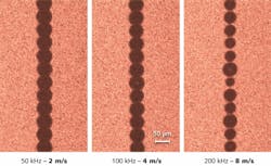
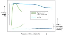
Increasing the beam scanning speed is the alternative approach. This requires higher laser pulse repetition frequency (PRF) so the proper pulse-to-pulse overlap can be maintained along the scribe line at the higher speed. Until recently, however, Q-switched DPSS laser pulse characteristics have deteriorated at very high repetition rates. In a typical laser, as PRF reaches beyond about 100 kHz, power drops off significantly and pulse-to-pulse energy variability increases substantially. This leads to unacceptable variations among the individual ablation spots (see Fig. 1). The P2 scribes shown are acceptable at 2 and 4 m/s scribing speeds. As PRF is increased to 200 kHz to enable a scribing speed of 8 m/s, pulse-energy fluctuations yield variations in the ablated spot size, and failure of adjacent pulses to overlap ensues. Ultimately, the result is a poorly performing solar panel.A new laser promises throughput improvement
Recognizing the need for TFPV scribing as well as other micromachining processes to be implemented at higher operating PRFs, we have developed the Mosaic 532-11 laser. Its 532 nm wavelength is ideally suited to the P2 and P3 scribing steps for a-Si and CdTe solar panels, and can also be used for the P1 scribe. The laser bundles an array of proprietary technologies into a platform that addresses market pressure for higher-throughput TFPV scribing at a lower cost. The Mosaic offers higher average power and low pulse-to-pulse energy variability at very high PRFs (see Fig. 2). In the regime well above 100 kHz, Mosaic opens up the possibility of process speeds that previously have not been possible with typical Q-switched DPSS lasers. At 200 kHz and 8 m/s, pulse-to-pulse variation of ablated spot size is eliminated and overlap is repeatable at all points along the scribe (see Fig. 3). This ensures the rigorous process control that TFPV scribing demands to avoid process variations that diminish the solar panel’s energy conversion efficiency.Rapid advances in PV manufacturing processes and equipment are in evidence as techniques such as laser scribing emerged from the lab and were optimized so manufacturing floor implementation became economically viable. The drive toward grid parity will motivate further optimization of TFPV laser scribing and the laser engines at the heart of the process. Innovative laser designs that expand the operating envelope to higher PRFs will be an important part of the technology’s full maturation. Results of our test shows that scribe speeds of more than 4 m/s with the current generation of DPSS Q-switched lasers operating at >100 kHz, while still maintaining continuous isolation scribes, is not possible due to higher pulse-to-pulse energy variability. Higher output power and lower pulse-to-pulse variability in new high-PRF regimes provide one path to improve speed and quality of the TFPV scribing process, which can help improve yield and reduce overall cost of TFPV manufacturing. New lasers that enable stable, reliable high-PRF operation will benefit other advanced industrial processes where narrow, clean, highly precise lines must be drawn, scribed, or cut, with the quality and repeatability we have come to expect from laser micromachining.
REFERENCES
1. A.D. Compaan, “Laser processing for thin-film photovoltaics,” Proc. SPIE, 2403, 224 (1995).
2. S. Haas et al., “High speed laser processing for monolithic series connection of silicon thin-film modules,” Prog. Photovolt: Res. Appl., 6, 195–203 (2008).
3. C.M. Dunsky and F. Colville, “Solid State Laser Applications in Photovoltaics Manufacturing,” Proc. SPIE, 6871, 687129-1 (2008).
4. J. Bovatsek et al., “Thin film removal mechanisms in ns-laser processing of photovoltaic materials,” Thin Solid Films, 518, 2897–2904 (2010).
About the Author
Rajesh Patel
Independent Consultant
Rajesh Patel, now an independent consultant in laser applications, was with MKS Spectra-Physics from 2006 through 2018, with his most recent role there being Director of Strategic Marketing and Applications Engineering.
Jim Bovatsek
Jim Bovatsek is a senior manager of applications engineering at MKS Spectra-Physics industrial applications laboratory in Milpitas, CA. He has focused on laser applications development using nanosecond, picosecond, and femtosecond pulsed lasers since 2000, with various publications and patents having been generated. He holds a Bachelor of Science (Physics) degree from the University of California, Santa Barbara.
Herman Chui
Vice President & General Manager, MKS Spectra-Physics
Herman Chui is Vice President & General Manager, Photonics Solutions Division, Lasers at MKS Spectra-Physics (Milpitas, CA).
Tim Edwards
Senior Manager, Product Marketing, MKS Spectra-Physics
Tim Edwards, now Owner of Technical Growth Marketing, LLC, was Senior Manager of Product Marketing at MKS Spectra-Physics (Milpitas, CA) from 2008 through 2011.


