The semiconductor industry's pursuit of miniaturization has pushed linewidths on integrated-circuit (IC) chips down to 100 nm. To pattern ever-finer lines by use of photolithography, the industry is now making the transition from krypton-fluoride (KrF) excimer-laser light sources emitting at 248-nm to argon-fluoride (ArF) lasers, which deliver 193 nm. Within a few years, even the ArF wavelength will be too long and fluorine (F2) lasers at 157 nm will be needed, bringing with them serious materials challenges, as most common optical materials do not transmit at this wavelength. Beyond fluorine lies the leap to extreme ultraviolet (EUV) at 13 nm. Whether lasers will be used to produce this short-wavelength radiation by the end of the decade is anybody's guess.
From KrF to ArF
The wavelength of the laser light source for lithography determines the width of the smallest line that can be formed on a wafer. Semiconductor processors use DRAM (dynamic random-access memory) half-pitch as a measure of the linewidth. Roughly speaking, the minimum linewidth possible is just half the wavelength of the laser light used (see also "Improving performance with MOPA"). At the moment, the mature technology for microcircuit lithography is based on KrF lasers operating at 248 nm. Light from these lasers can be focused with ordinary fused-silica optics and can produce linewidths as fine as 130 nm.
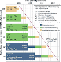
The industry is racing to complete the transition to the next level down, using ArF lasers operating at 193 nm. These have to be in place on the manufacturing line by 2003 to produce chips with 90-nm linewidths. The increasing challenges of lithography are likely to mean that IC linewidths will shrink at a rate of no greater than 50% every two years, according to the International Technology Roadmap of Semiconductors (ITRS), the industry-wide plan for technological progress (see Fig. 1).1
One of the challenges in moving from KrF to ArF is that fused silica has some absorption at 193 nm. Another optical-material option, calcium fluoride (CaF2), is highly transparent at that wavelength. While fused-silica lenses have been used for decades for UV applications, CaF2 lenses are a much less mature technology still bedeviled by issues of yield, cost, and quality. Calcium fluoride also has a much higher coefficient of thermal expansion than quartz. To avoid some of the problems associated with CaF2, Corning (Ithaca, NY) has started production of ultrahigh-transmission fused-silica glass that could be used for ArF lenses. An additional challenge facing the industry is wafer and mask inspection (see "UV laser light reveals killer defects").
The problems facing developers of ArF technology were illustrated dramatically in July 2001, when Intel (Santa Clara, CA) scrapped plans to buy $100 million worth of 193-nm lithography tools from Silicon Valley Group, a subsidiary of ASM Lithography (Veldhoven, the Netherlands). The cancellation was caused by repeated delays in the delivery of the tools as a result of difficulties with the lenses, photoresists, and masks. Instead, Intel pushed back to early 2003 production runs with ArF technology.
On to fluorine
Because the difference in wavelength between KrF and ArF is only 28%, the transition will only buy the semiconductor processor two years before even shorter wavelengths are needed. The fact that the large investment in ArF technology research, development, and manufacturing must be paid back in roughly two years is putting IC chipmakers under intense financial pressure.
Nonetheless, the industry is already well into preparations for the next transition. By 2006 or 2007, ArF lasers will have to be replaced by 157-nm-emitting F2 lasers. This change will make possible 65-nm linewidths and chip densities four times as high as those currently in production. But 157-nm optics are even more difficult than those at 193 nm. While CaF2 can still be used for lenses, an increase in both quality and quantity of material is required at the shorter wavelengths. However, advanced fused silica could be a real alternative by that time.2 Another problem is that oxygen, water, and carbon dioxide molecules all strongly absorb 157-nm light, so nitrogen purging must be used to keep these absorbing gases at a part-per-million level or below.
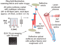
At less than 157 nm, a combination of lasing materials, refractive lenses, and photoresists just does not exist. The next jump in technology will almost certainly be to EUV in the 13-nm range. The need for this wavelength is defined by the capabilities of the multilayer mirrors used for focusing. Focusing such short-wavelength radiation is a challenge (see Fig. 2). The photomasks work in reflection and consist of a multilayer reflecting substrate with a patterned absorbing layer. While the masks can be patterned with conventional technology, the multilayer substrate is almost impossible to repair, so a complete lack of defects is essential.Lasers and EUV
It is likely, but not certain, that lasers will be involved in the production of EUV radiation. In one scheme, light from a KrF laser is focused on a supersonic stream of xenon gas, which then reradiates a small part of the energy in broad bands around 11 and 13 nm. But the low density of the gas leads to a low conversion efficiency and the cool gas surrounding the laser-heated spot will absorb some of the EUV radiation produced. There are ideas to minimize hese problems such as by using a buffer gas that surrounds the xenon and compresses it (see Fig. 3).3Several nonlaser methods exist for producing EUV radiation but a new technology will not be needed for chip production before the end of the decade; advances in optical techniques might push it off as far as 2013. But decisions on which route to choose will probably have to be made considerably earlier, perhaps by the end of 2004, according to the ITRS plan. By that time it will be clear whether lasers will continue to be central to semiconductor manufacture or will be superceded by other technologies.
REFERENCES
1. See http://public.itrs.net/Files/2001ITRS/Home.htm.
2. J. Mulkens et al., SPIE 3873, 372 (July 2000).
3. R. De Buruijn et al., SPIE 3997, 157 (February 2001).


