Photonics West Preview: SPIE Photonics West 2015 excites with neurology, 3D printing, and silicon photonics
SPIE Photonics West has always been the go-to conference for new and exciting technological breakthroughs in the field of photonics. This year, as we enter the 2015 International Year of Light, SPIE Photonics West takes a more detailed look at neurology, 3D printing, and silicon photonics—some of the hottest buzzwords and buzz phrases in the photonics industry today—that have vast, far-reaching implications for the future of our society.
Imagine being able to probe, study, and even modify the brain’s behavior using light (can you say “optogenetics”?). Now envision using light to print brain matter and other biological tissues for life-saving repairs and mind-altering benefits (are you thinking “3D printing”?). And finally, imagine using light to communicate faster than ever before using ultra-tiny circuits that circumvent cumbersome, bulk-optic devices and interconnect bottlenecks with faster-than-light photonic circuitry (have you heard of “silicon photonics”?).
These and numerous other wonders of the photonics world are hurtling toward you at SPIE Photonics West 2015 (with 8% more technical papers than last year) from February 7 to 12 in San Francisco. These wonders take the form of plenary sessions, papers, exhibits, and restaurant conversations with photonic gurus and wanna-be gurus hungry to learn more about how photonics can positively impact our world.
“With the recent commitment of more funds toward the White House BRAIN Initiative and experts coming to Photonics West from all over the world—including several from the Britton Chance Center for Biomedical Photonics at the Wuhan National Lab for Optoelectronics—presentations will represent not only the latest work, but a heightened sense of direction and drive,” says SPIE public relations manager Amy Nelson. “Integrated photonics for next-generation computing is an important area to watch as well, and speakers from companies including IBM, Intel, and Corning will be among those presenting their latest work and directions.
“Translational research has been quickly adopted by those in the biomedical optics community looking for ways to speed the delivery of new treatments and diagnostic methods to the patient, and the number of papers in the program has increased this year,” says Nelson. “The Green Photonics program continues to dazzle with research that will enable applications in more efficient photovoltaics, more disaster-resistant telecommunications systems, and new solid-state lighting solutions for the developed as well as the developing world.”
And once again, SPIE brings in the heavy hitters with several plenary, keynote, and invited talks to be given by Nobel Laureates: Eric Betzig and William Moerner will speak about their prize-winning work in the field of microscopy (search on their names at http://www.spie.org/photonics-west.xml to bring up the presentations); Shuji Nakamura will address the SPIE Fellows luncheon (see http://spie.org/PW/specialevents/Membership-Event); Thomas Südhof will give the Neurophotonics plenary on Tuesday (February 10, 2–3 pm), a new plenary area this year; and Kostya Novoselov, Isamu Akasaki, Hiroshi Amano, and Shuji Nakamura are all authors of papers being presented.
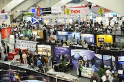
“The SPIE Photonics West Exhibition is sold out for 2015 with all available space currently committed and a waiting list in place,” says Peter Hallett, SPIE director, marketing and industry relations. “Approximately 1250 suppliers, developers, and manufacturers of the latest products, tools, and applications for research and industry will be on the floor.” Hallett adds, “This year, 13 international cluster and 4 U.S. regional cluster booths are participating, including new-in-2015 pavilions from Taiwan, Austria, and Korea that make SPIE Photonics West a true global marketplace where people can speak face-to-face with the best suppliers from around the world.”
And last but not least, please attend the SPIE Photonics West welcome reception on Monday, February 9 from 7 to 8:30 pm. With the theme of the reception being “Creatures of the Light” in the 2015 International Year of Light, how can you go wrong? SPIE says it will take a “creative look backward to the beginnings of time when light was all we had.”
BiOS and Translational Research virtual symposium
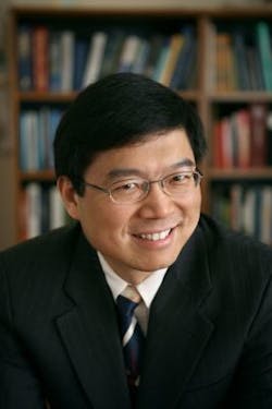
The Biomedical Optics Symposium (BiOS) and BiOS Expo will open Photonics West on Saturday, February 7. BiOS is organized into five tracks, including Photonic Therapeutics and Diagnostics; Clinical Technologies and Systems; and Nano/Biophotonics. Each of the other two tracks is a mouthful: Tissue Optics, Laser-Tissue Interaction, and Tissue Engineering; and Biomedical Spectroscopy, Microscopy, and Imaging. In addition, Translational Research is a virtual symposium that includes BiOS presentations in all five tracks—on technologies, tools, and techniques that show high potential to improve healthcare practice.If past years are any indication, even after a full day exploring the conferences, exhibits, and interactive poster session, attendees will bring enthusiastic attention to the Saturday Hot Topics plenary (7–9 pm). Hot Topics will begin with presentation of SPIE’s 2015 awards in biomedical optics, including the Biophotonics Technology Innovator Award (as of late November, the winner had not been announced) and the Britton Chance Biomedical Optics Award, which will honor Lihong Wang of Washington University (St. Louis, MO) for “outstanding lifetime contributions” (see Fig. 1). Wang is being recognized for his pioneering technical work and visionary leadership in the development and application of photoacoustics and photon transport modeling; he will deliver a talk titled “Photon-Phonon Synergy: Photoacoustic Tomography and Beyond.”
The remaining talks will cover advances in imaging: Brett Bouma of the Wellman Center for Photomedicine will report on endoscopic OCT, Richard Rosen of the New York Eye and Ear Infirmary will describe adaptive optics for the retina, MIT’s Peter So will report on nonlinear microscopy, and Rafael Yuste of Columbia University will describe simultaneous imaging of neural activity in 3D (at the 2014 Hot Topics session, Yuste, a pioneer behind the U.S. Brain Research through Advancing Innovative Neurotechnologies (BRAIN) Initiative, explained why optical imaging is key for neuroscience).
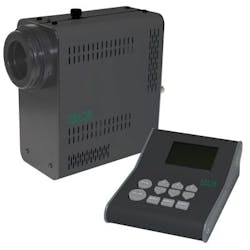
Sunday, February 8 will see the continuation of BiOS Expo, which will feature more than 210 exhibitors with products such as advanced microscopes, analytical instruments, nanosecond lasers, fiber optics, spectral sensing systems, and scientific cameras. Many new products will be on display such as Prior Scientific’s (Rockland, MA) Lumen 300-LED broad spectrum white light fluorescence excitation illumination system (see Fig. 2). Other product introductions are a developer’s kit for FEMTOprint SA’s (Muzzano, Switzerland) tabletop platform for making 3D micro-nanodevices; a free-running single-photon detector for the near-IR range from ID Quantique (Geneva, Switzerland); and Raptor Photonics’ (Larne, Northern Ireland) cooled visible-SWIR InGaAs camera. In case you don’t get to see all the vendors you want to on Saturday and Sunday, keep in mind that some will also exhibit in the Photonics West Expo starting Tuesday.Two special events are set to begin Sunday at 12:30: the BiOS Student Networking Lunch with the Experts and the Translational Research Lunchtime Forum. The latter will feature Bruce Tromberg of UC Irvine and Gabriela Apiou of Harvard Medical School facilitating a discussion about outcomes-based work that can change the lives of patients, presentations of work selected from the Translational Research virtual symposium, and Best Paper awards.
Then, from 5–7 pm on Sunday, academic researchers and those working in small business will have an opportunity to learn about U.S. Food and Drug Administration (FDA) policies and procedures relevant to their work. Chaired by Warren Grundfest of UCLA and Ramesh Raghavachari of the FDA, the session will feature Roger Bagwell of Actuated Medical offering insights on regulatory approval and commercialization of medical devices, and Martin Culjat of Farus LLC and UCLA on FDA submissions for startups. At 7 pm, Nobel Laureates Betzig and Moerner talk about their work on fluorescence microscopy as described in the introduction to this preview.
On Monday, February 9, three prizes will be awarded to early career scientists with the JenLab Young Investigator Award (9:35 am) and the Student Poster Session Competition (2:50 pm), both of which are part of the Multiphoton Microscopy in the Biomedical Sciences conference, and the Ocean Optics Young Investigator Award (6:10 pm), in conjunction with the Colloidal Nanocrystals for Biomedical Applications conference. (Two other awards programs, the PicoQuant Young Investigator Award, part of the Single Molecule Spectroscopy and Superresolution Imaging conference, and the Seno Medical Best Paper Awards, part of the Photons Plus Ultrasound conference, run on Sunday at 3:25 pm and Tuesday at 5:40 pm, respectively).
Three more plenary sessions will take place on Tuesday, February 10. In the Nano/Biophotonics plenary (10:30 am), Gabriel Popescu of the University of Illinois at Urbana-Champaign will discuss the use of optics to bridge molecular and cellular biology and present some recent advances in phase-sensitive measurements. The Neurophotonics plenary (2 pm), delivered by 2013 Nobel Laureate Thomas C. Südhof of the Stanford University School of Medicine, will describe recent studies showing how dysfunction of neurexins and their ligands might predispose to neuropsychiatric disorders. And the evening plenary, hosted by the International Biomedical Optics Society group—which aims to facilitate communications between clinicians and engineers—will feature a talk by Stephen Boppart of the University of Illinois at Urbana-Champaign: Transforming Medicine and Surgery with Biophotonics.
BiOS interactive poster sessions will run through Tuesday (hours are Saturday and Sunday, 3–4 pm, Sunday and Monday, 5:30 – 7:30 pm, and Tuesday, 6–8 pm), and the BiOS conferences will run through Thursday. While it is difficult to select highlights from the thousands of fascinating offerings, here are a few that captured our attention. The first three are part of the Translational Research virtual symposium:
1. Paper 9303-603: Photoacoustic imaging: A potential new platform for assessment of bone health (a technologically difficult task), by Xueding Wang of the University of Michigan Medical School and colleagues.
2. Paper 9308-18: Enabling technology for photodynamic therapy in global health settings: Battery-powered irradiation and smartphone-based imaging for ALA-PDT by Joshua Hempstead of the University of Massachusetts (Boston) and colleagues. Photonics has much to offer global health, and this is an exciting new example.
3. Paper 9311-7: Quantitative wide-field fluorescence imaging in neurosurgery by Keith Paulsen of the Thayer School of Engineering at Dartmouth College and colleagues. Wow: fluorescence-guided neurosurgery.
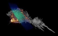
4. Paper 9334-22: Lattice light-sheet microscopy: Imaging molecules, cells, and embryos at high spatio-temporal resolution by Wesley Legant, Howard Hughes Medical Institute, Janelia Farm Research Campus and colleagues. This technique represents recent work by Nobel Laureate Betzig (see Fig. 3).LASE
The LASE plenary session, held Wednesday, includes presentations on the future of NASA’s optical communications program by Donald Cornwall Jr., head of NASA’s Advanced Communications Division; coherent combination of ultrafast laser pulses by Jens Limpert, head of the Laser Development Group at Friedrich-Schiller-Universität Jena (Germany); and laser 3D printing of metallic components by Xiaoyan Zeng, deputy director of the lasers and terahertz department at Wuhan National Laboratory for Optoelectronics (China). The talk given by Limpert is notable in that he discusses the coherent combination of a large number of ultrafast fiber amplifiers, with the goal of not only petawatt peak powers, but also megawatt average powers.
The LASE technical sessions are divided into five tracks: Laser Source Engineering, Nonlinear Optics, Semiconductor Lasers and LEDs, Laser Micro-/Nanoengineering, and Laser Applications. A few of the almost 30 technical-session topics include Fiber Lasers XII: Technology, Systems, and Applications (Conference 9344); Ultrafast Phenomena and Nanophotonics XIX (Conference 9361); High-Power Diode Laser Technology and Applications XIII (Conference 9348); Advanced Fabrication Technologies for Micro/Nano Optics and Photonics VIII (Conference 9374); and Laser Refrigeration of Solids VIII (Conference 9380). And, of course, each of these 30 session topics has its own group of subtopics, resulting in hundreds of individual session tracks—surely one for every researcher’s and engineer’s specialty.
In a session on the integration of nanostructures into photovoltaics (9352-13; Sunday, February 8), Vivian Ferry of the University of Minnesota (Minneapolis) discusses the many ways that nanostructures offer the ability to control, concentrate, and spectrally tune light in subwavelength dimensions; the talk concentrates both on light trapping and luminescent solar concentrators.
The use of fiber lasers as directed-energy devices will be the topic of an invited paper (9344-12; Monday, February 9) by Don Seeley of the High Energy Laser Joint Technology Office (HEL-JTO; Kirtland AFB, NM) and John Slater and LeAnn Brasure of Schafer Corp. (Arlington, VA). The same session track includes a talk on extreme-ultraviolet generation by a high-intensity nanosecond all-fiber-coiled laser, given by Chun-Lin Chang and colleagues from National Taiwan University and National Central University (Taiwan).
A multinational team of researchers will describe the achievement of 517–538 nm tunable second-harmonic generation in a diode-pumped periodically poled potassium titanyl phosphate (PPKTP) waveguide crystal (9347-11; Tuesday, February 10) using a tunable quantum-well (QW) external-cavity fiber-coupled laser diode; maximum output power at 530 nm is 12.88 mW. On Wednesday, February 11 (paper 9353-15), a German group will discuss the direct laser writing of 3D nanostructures using a 405 nm laser diode; the shorter wavelength allows them to create periodic structures with a finer lattice constant.
In an invited paper (9363-56; Thursday, February 12), a group from Nichia (Anan, Japan) will present recent results on high-output-power deep ultraviolet LEDs emitting, for example, 35 mW at 258 nm for a single-chip device with a lifetime of more than 3000 h. Researchers at Korea University (Seoul) will discuss the use of chemically doped graphene films as a transparent conductive layer in gallium nitride (GaN)-based LEDs (9363-75; Thursday, February 12); such layers can replace the fragile indium-tin-oxide layer currently widely used. Experimental results will be presented.
OPTO
Held on Monday, February 9, the OPTO plenary session will open with a talk on silicon integrated nanophotonics given by Yurii Vlasov of the IBM Thomas J. Watson Research Center (Yorktown Heights, NY). Vlasov will highlight IBM’s nanophotonics technology for cost-efficient optical links that connect racks, modules, and chips together with ultralow-power single-die optical transceivers. Christoph Lienau from Carl von Ossietzky Universität Oldenburg (Germany) will discuss ultrafast coherent charge transfer in solar cells, using coherent femtosecond spectroscopy for exploration at the tens-of-femtoseconds time scale. Harry Atwater from the California Institute of Technology (Caltech; Pasadena) will highlight progress in tunable and quantum metaphotonics (resonant subwavelength structures), which can serve as tunable radiation absorbers or emitters.
The OPTO session tracks cover the gamut, including Optoelectronic Materials and Devices; Photonic Integration; Nanotechnologies in Photonics; MOEMS-MEMS in Photonics; Advanced Quantum and Optoelectronic Applications; Semiconductor Lasers and LEDs; Displays and Holography; and Optical Communications: Devices to Systems. Integrated photonics and nanotechnology are both hot topics that appear repeatedly in these sessions.
For example, researchers from the University of Twente (Enschede, The Netherlands) will describe the fabrication and testing of spiral-waveguide amplifiers in erbium-doped aluminum oxide on a silicon chip (9365-21; Tuesday, February 10); the devices show an internal net gain of 20 dB at 1532 nm. A group at Fachhochschule Karlsruhe Technik und Wirtschaft (Karlsruhe, Germany) will discuss air-suspended quasi-singlemode polymer rib waveguides (9365-28; Tuesday, February 10); suspending waveguides in air results in air cladding that produces the highest refractive-index contrast possible between the core and cladding.
Scientists from Caltech and the Jet Propulsion Laboratory (Pasadena, CA) will present the development of efficient high-numerical-aperture flat microlenses made from high-contrast “transmit arrays,” which are a periodic arrangement of amorphous-silicon posts with different diameters on a fused-silica substrate (9372-24; Thursday, February 12). The near-infrared microlenses have spot sizes as small as 0.57 λ and focusing efficiencies of more than 80%.
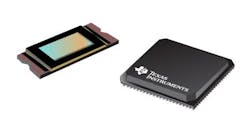
One of the most common microelectromechanical-systems (MEMs) devices, the digital micromirror device (DMD), is the topic of its own group of sessions. In one example, a group of French astrophysicists will present results on a DMD-based programmable wide-field spectrograph for Earth observation (9376-16; Wednesday, February 11); the DMD tailors the spectrum of the spectrograph. A mockup has already been designed, fabricated, and tested. Bjarke Rose of Ibsen Photonics (Farum, Denmark) will discuss programmable spectroscopy enabled by a digital light projector (DLP; see Fig. 4), as opposed to more-traditional diode-array-based spectrometers (9376-18; Wednesday, February 11).Green Photonics virtual symposium
Once again chairing the Green Photonics virtual symposium, Steve Eglash, executive director of the Stanford Data Science Initiative at Stanford University, sees two OPTO plenary talks of particular interest: “Silicon integrated nanophotonics: From fundamental science to manufacturable technology” from Yurii Vlasov of the IBM T.J. Watson Research Center (February 9, 8:10–8:50 am) and “Ultrafast coherent charge transfer in solar cells and artificial light harvesting systems: Toward movies of electronic motion” from Christoph Lienau of Carl von Ossietzky University (February 9, 8:50–9:30 am).
Eglash says the Green Photonics symposium highlights papers from OPTO and LASE that show how new photonic and optoelectronic tools and materials will reduce power consumption, enable cleaner manufacturing, and generate new energy for a broad range of applications. Papers describe progress and breakthroughs in biomedicine, photovoltaics (PV), solid-state lighting (SSL), battery manufacturing, optical communications (at all scales from intra-chip to intercontinental), optical characterization/spectroscopy/metrology, and sensors for the Internet of Things and applications such as climate-change adaptation.
Among labs reporting on advances in nanophotonics toward improved PV efficiency are Fraunhofer IWS describing a new generation of thin metallic films in fabricating highly efficient transparent electrodes without the use of rare earth materials (paper 9351-41), and the University of Minnesota, Twin Cities, where researchers are working to increase absorption in semiconductor films to enhance performance and decrease production cost. Light is trapped in ultrathin silicon solar cells with metallic and resonant semiconductor nanostructures (paper 9352-13).
Eglash adds that efficient new light sources will provide long-lived and economical illumination for human activities and information display. Researchers at the Technische Universität Braunschweig (Germany) describe GaN nanorods and 3D columns as an exciting new route toward light engines for SSL (paper 9383-38), and a team from National Taiwan University will report on using cholesteric liquid crystals for a long-lived bright light source without the need for continuously supplied voltage (paper 9384-26).
Photonics are at work in disaster prevention and management as well. A team from the National Institute of Information and Communications Technology in Japan will report on a wireless mesh network test demonstrating disaster-resistant telecommunication technologies (paper 9387-19). Also, anticipating climate-change related floods and landslides, researchers from the Universidad Pontificia Bolivariana (Columbia) will report on a hybrid optical and wireless sensor network with highly reconfigurable and self-healing capabilities (paper 9387-22).
About the Author

Gail Overton
Senior Editor (2004-2020)
Gail has more than 30 years of engineering, marketing, product management, and editorial experience in the photonics and optical communications industry. Before joining the staff at Laser Focus World in 2004, she held many product management and product marketing roles in the fiber-optics industry, most notably at Hughes (El Segundo, CA), GTE Labs (Waltham, MA), Corning (Corning, NY), Photon Kinetics (Beaverton, OR), and Newport Corporation (Irvine, CA). During her marketing career, Gail published articles in WDM Solutions and Sensors magazine and traveled internationally to conduct product and sales training. Gail received her BS degree in physics, with an emphasis in optics, from San Diego State University in San Diego, CA in May 1986.
John Wallace
Senior Technical Editor (1998-2022)
John Wallace was with Laser Focus World for nearly 25 years, retiring in late June 2022. He obtained a bachelor's degree in mechanical engineering and physics at Rutgers University and a master's in optical engineering at the University of Rochester. Before becoming an editor, John worked as an engineer at RCA, Exxon, Eastman Kodak, and GCA Corporation.

Barbara Gefvert
Editor-in-Chief, BioOptics World (2008-2020)
Barbara G. Gefvert has been a science and technology editor and writer since 1987, and served as editor in chief on multiple publications, including Sensors magazine for nearly a decade.
