Photonics Products: Microscopes: Industrial microscopes aid precision manufacturing
While microscopes are an essential research tool in biology and other sciences, they are just as needed in industry, where fine manufacturing tolerances necessitate microscopic vision for many tasks. Industrial microscopes come in configurations that are as varied as the tasks they accomplish.
Decisions to be made when selecting a microscope include whether to go for a general-purpose instrument or one tailored to one specific task, low- or high-power magnification or both, visual or (more likely) camera-based imaging, manual or automated hardware, what wavelength range is best for the job, and, of course, finding the right balance between economy and capability.
Versatility
Many microscope manufacturers produce a variety of general-purpose microscope equipment from which the user picks and chooses hardware as one way of customizing the instrument for his or her purposes, with fully customized systems another option. For example, Santa Barbara Imaging (Goleta, CA) makes microscopes that serve in low- to high-magnification applications with fields of view from 30 mm down to 50 μm.
The company's low-magnification microscopes are available in fixed or variable-zoom magnification; illumination is typically a ring light or goose-neck lamp. High-magnification microscopes are the infinity-corrected type and are supplied with integrated coaxial LED illumination, a C-mount for the imager, and a threaded insert for the objective. All systems use an imager and monitor or computer to provide the object display (no eyepieces).
"The low-magnification microscopes are typically used in assembly and inspection applications such as fine connector soldering and quality inspection or small machined parts inspection," says Jeff Markakis, a design engineer for Santa Barbara Imaging. "The high-magnification microscopes are typically used in embedded applications such as semiconductor inspection, semiconductor bonding, single-use medical-applicator inspection, surface-treatment qualification, and fine parts alignment."
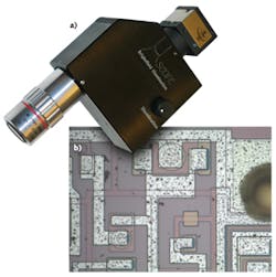
In one example, the company's μScope is a compact, infinity-corrected, single-objective microscope with integrated coaxial LED illumination intended for dedicated applications. The instrument has a motorized cross-roller focus stage with a 50 mm focus travel range, submicron positioning, stepper-motor drive, and an integrated stepper-motor controller (see Fig. 1). Nanotronics Imaging (Cuyahoga Falls, OH) makes a variety of configurable industrial-grade optical microscopes constructed primarily from off-the-shelf components. Its microscopes have been used in cancer research labs, medical-testing labs, and semiconductor research labs, as well as production facilities, says Jacobs Keith, an engineering technologist at Nanotronics. He says that the company aims to "provide all the bells and whistles of multimillion-dollar inspection tools, complete with automated cassette and wafer handling, OCR integration, and wafer alignment."
Automation is important, he adds, noting that in addition to providing automation hardware with its own microscopes, Nanotronics works with customers to outfit their existing manual microscopes with automated systems. The company can also provide atomic-force microscopes (AFMs) in addition to optical microscopes.
Nanotronics' nSPEC microscope acquires its images via scanning with an integrated laser system over user-selected areas. Image-processing software is then used to identify and classify micron-sized and larger defects; the results are exported using industry-standard protocols. Many types of operation are supported, including transmission, bright-field, dark-field, differential-interference contrast (DIC), epifluorescence, and polarized-light measurements.
The company's production-line microscope is equipped with robotic wafer handling for 2, 4, 6, and 8 in. wafers, a wafer-flat or notch alignment mechanism, automated stages, and real-time laser autofocus, and can read optical character recognition (OCR) codes on the backs or fronts of wafers. Along with standard image collection, it can run time-lapse photography over specified locations. (The microscope is also used in the biomedical arena, for example, to distinguish between cancerous and healthy cells.)
"It is difficult to believe," says Keith, "but even today in the high-tech industry of semiconductor research and manufacturing, a surprising percentage of inspection is still performed by rows of dozens or even hundreds of technicians manually inspecting each and every wafer that flows through a production facility. As you can imagine, an automated system can inspect a wafer without tired eyes and dulled senses from hours staring through a microscope."
Metrology
The ever-growing need for ultraprecise 3D noncontact surface inspection and metrology has pushed microscope hardware and software development, allowing the measurement and calculation of such surface parameters as root-mean-square (RMS) surface height, degree of symmetry of surface height (skewness), "peakedness" of surface height, surface slopes, spatial frequency distribution, and others (see Fig. 2).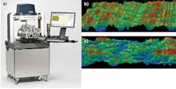
For example, interferometric microscopes produced by Bruker (Billerica, MA) can measure surface height to subnanometer resolution—useful in industries such as medical, automotive, aerospace, electronics, solar, microelectromechanical systems (MEMS) manufacture, data storage, general manufacturing, and precision machining.
Bruker's 3D optical microscopes combine 64-bit multicore operation-analysis software with white-light-interferometric hardware to provide angstrom-to-millimeter vertical-range metrology over large fields of view; Bruker's systems range from benchtop instruments to fully automated multiple-objective systems with integrated isolation tables and self-calibration for production-floor use.
"Common applications include automotive components, precision machined surfaces, optics/optical systems, MEMS, thin and thick films, semiconductors, data-storage components, and medical devices," notes Steve Hopkins, marketing communications supervisor at Bruker.
The company's NPFLEX 3D optical microscope is intended for surface measurement of large samples such as orthopedic medical implants and large and unusual parts routinely seen in the aerospace, automotive, and precision machining industries. The system has an open-gantry design that allows 300° of access to surfaces, handling microscopic to macroscopic features on samples with sizes up to 13 in. tall. The option of a swiveling optical head allows investigation of highly curved samples and beveled edges, while an objective crash-mitigation system eliminates potential contact damage.
Olympus (Tokyo, Japan) has been producing microscopes since its formation in 1919. The company makes industrial microscope systems for optical metrology and imaging applications; its instruments range from basic stereo microscopes, compound microscopes, and inverted microscopes to advanced optical-digital microscopes.
Uses of the company's instruments include manufacturing, metal and alloy analysis, alternative energy, aerospace, automotive, high-level quality assurance and quality control, surface metrology/inspection, grains analysis, and particle inspection, according to David Rideout, marketing manager at Olympus.
A laser scanning confocal microscope made by Olympus, the LEXT OLS4100, allows noncontact 3D observation and measurement of surface features to a 10 nm resolution, says Rideout. The instrument is based on a dual confocal system that captures images from samples consisting of materials with differing reflectance characteristics.
In addition to laser imaging, the microscope uses a white LED light and a high-color-fidelity CCD camera to generate color images that can be overlaid upon the 3D laser image for a 3D sample representation. Objective lenses with high numerical apertures and an optical system designed for the microscope's 405-nm-emitting laser allow the microscope to measure acute-angled samples, as well as microroughness on uneven surfaces. Applications include the manufacture of semiconductor components, flat-panel displays, and MEMS, as well as materials processing.
Automation
While a number of microscope makers provide varying levels of automation hardware and software with their equipment, Prior Scientific (Cambridge, England) is entirely devoted to producing automation components and systems.
An entire category of microscope stages, the HT series, was developed by Prior Scientific specifically for hardness testing and other high-load applications, says John Commesso, who does marketing and advertising for the company. These stages have travel ranges of up to 250 × 150 mm and load capacities up to 100 kg, helping hardness-testing instruments to counter the high point loads produced while testing metallic samples and enabling them to produce a precise pattern of indentations on a sample and, in conjunction with imaging software, to produce a hardness map.
Motorized stages from Prior can be used with microscopes to automatically determine the consistency of thin films ranging from nanometers to microns thick; here, measuring film thickness requires collecting the interference pattern from a sample. These measurements are used to check film thickness on optics, semiconductor devices, and thin-film photovoltaics as well as other devices.
In Fourier-transform IR (FTIR) spectroscopy, absorption measurements of spectra either reflected off or transmitted through a material sample, are compared to libraries of known materials, allowing the test material to be identified. Microscope stages and focus devices are used for automated scanning here also, says Commesso.
For general inspection, the extended-depth-of-field (EDF) technique, in which focus motors and stages are used along with a camera and optics to capture a stack of images at different focus positions, enables the user to display the stack of images as a composite, effectively creating a 3D image. Industrial uses of EDF techniques can involve use with metallurgical microscopes to analyze material stress, strain, and fatigue. Other EDF applications using microscope stage automation include 3D surface imaging, surface topography, crystallography, and weld inspection.
Commesso notes that Prior Scientific's x-y stages, combined with software tools, can "stitch" together multiple images taken at higher magnifications to create a high-resolution mosaic image for examining parts that are larger than a microscope's field of view. High-resolution images help to locate and identify defects, as well as measure angles and radii in processes ranging from high precision machining to nanomanufacturing.
Company websites:
Santa Barbara Imaging: www.santabarbaraimaging.com
Nanotronics Imaging: www.nanotronicsimaging.com
Bruker: ww.bruker.com
Olympus: www.olympusamerica.com
Prior Scientific: www.prior.com
About the Author

John Wallace
Senior Technical Editor (1998-2022)
John Wallace was with Laser Focus World for nearly 25 years, retiring in late June 2022. He obtained a bachelor's degree in mechanical engineering and physics at Rutgers University and a master's in optical engineering at the University of Rochester. Before becoming an editor, John worked as an engineer at RCA, Exxon, Eastman Kodak, and GCA Corporation.