LOW-LIGHT IMAGING: Scientific InGaAs FPA cameras heighten sensitivity for NIR imaging
Imaging and spectroscopy techniques performed in the near-infrared (NIR) or shortwave-IR (SWIR) region are playing an increasingly important role in many leading-edge scientific and industrial endeavors. For instance, investigations in this region are critical to research and development efforts to improve solar cells and semiconductors, advance the latest methods of photodynamic therapy, and develop a deeper understanding of stellar to geological landscapes via hyperspectral imaging.
Key to achieving higher sensitivity in the NIR range (0.9 to 1.7 μm) is the use of sensors based on indium gallium arsenide (InGaAs) focal-plane arrays (FPAs). An InGaAs FPA consists of a 2D photodiode array—itself comprising an indium phosphide (InP) substrate, an InGaAs absorption layer, and an ultrathin InP cap—that has been indium bump-bonded to a readout integrated circuit (ROIC).
In an InGaAs FPA, the 2D array detects incident light and then generates and collects charge; the ROIC clocks and converts the collected charge to voltage and transfers the resultant signal to off-chip electronics. InGaAs FPAs are typically back-illuminated and deliver excellent quantum efficiency (QE) in excess of 80%.
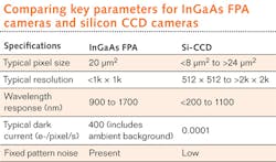
Currently, many life and physical science applications use silicon-based low-light-level CCD cameras for optical imaging and spectroscopy (see table). Although these Si-CCD cameras provide excellent QE in the ultraviolet-to-NIR range due to silicon's bandgap properties, even the best NIR-optimized CCDs cannot offer sensitivity beyond 1100 nm (see Fig. 1).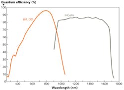
Scientific InGaAs FPA camera performance
Commercial NIR cameras incorporating InGaAs FPA sensors are typically designed for use in night-vision and thermal-inspection applications. Scientific applications, on the other hand, impose extreme demands on camera systems to achieve the best possible signal-to-noise ratio (SNR).
As discussed earlier, typical InGaAs FPAs have sensitivity between 900 and 1700 nm. However, great care must be taken to maximize photon collection before the incident light reaches the sensor. For instance, it is important to use a single optical window in the camera, treated with an antireflective (AR) coating to maximize photon throughput. One of the particularly noteworthy behaviors of InGaAs FPAs is that their long-wavelength cutoff is reduced when they are cooled. As a rule of thumb, the long-wavelength cutoff shifts by 8 nm for every 10°C of sensor cooling. This phenomenon can actually be advantageous, as the sensor is insensitive to background signal beyond the shifted far-end wavelength cutoff. In other words, the sensor acts like a "tunable" low-pass optical filter.
Due to a smaller bandgap, InGaAs FPAs are typically dark-noise-limited devices. For example, commercial InGaAs cameras only offer exposure times up to a few milliseconds, as the device saturates due to dark current. In contrast, the use of deep sensor cooling by scientific InGaAs cameras allows integration times of many seconds. Until recently, this deep cooling required liquid nitrogen; however, scientific InGaAs cameras can now achieve cooling down to -90°C via thermoelectric designs. It is important to note that the ambient dark background emission from the sample or experiment also contributes to the total dark noise of the detector, so care must be taken to keep the experiment as cold as possible.
Advanced camera designs also provide online correction for fixed pattern noise in InGaAs FPAs. This capability helps preserve uniformity across the dynamic range of the device.
Applications
Night vision and surveillance are traditionally the primary applications for commercial NIR detectors, but the availability of scientific-grade cameras with increased sensitivity is set to advance several key research and industrial applications.
In solar-cell inspection, photoluminescence (PL) imaging has great potential as an in-line monitoring tool. The ability to utilize this highly sensitive imaging technique during the early stages of the solar cell manufacturing process has significant ramifications, as PL images of ingots, bricks, and as-cut wafers can be predictive of final solar cell efficiency.
When 800 nm excitation light is applied to multicrystalline silicon (mc-Si) wafers, electron-hole pairs generated by light photons recombine, causing PL emission. In the band-to-band wavelength range (about 1000 to 1200 nm) for these wafers, the PL associated with defects (that is, impurities or anomalous material compositions) is weaker due to the recombination of relatively fewer electron-hole pairs in the flawed regions. Therefore, defects are perceived as darker in band-to-band PL images (see Fig. 2). In the defect-band wavelength range (about 1300 to 1600 nm), however, the defect-related sub-bandgap emissions are stronger. Therefore, defects are easier to observe in defect-band PL images. In both imaging methods, scientific InGaAs FPA cameras offer ideal response characteristics for PL imaging of mc-Si wafers. Most important, researchers have observed linear correlations between defect-band PL images from as-cut wafers (as well as from wafers after several other processing stages) and final solar-cell efficiencies.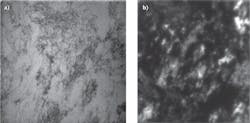
Other key applications of scientific deep-cooled, large-format InGaAs FPA cameras include nanotube fluorescence, emission, absorption, semiconductor-failure inspection, nondestructive testing, hyperspectral imaging, and singlet oxygen imaging.
REFERENCES
1. S. Johnston et al., "Imaging study of multi-crystalline silicon wafers throughout the manufacturing process," preprint, pres. at 37th IEEE Photovoltaic Specialists Conf. (PVSC 37), Seattle, WA, June 19–24, 2011.
2. F. Yan et al., "Defect-band emission photoluminescence imaging on multi-crystalline Si solar cells," preprint, pres. at 37th IEEE Photovoltaic Specialists Conf. (PVSC 37), Seattle, WA, June 19–24, 2011.
3. T. Trupke and W. McMillan, "Photoluminescence imaging speeds solar cell inspection," Laser Focus World, 46, 12, 35–41 (December 2010).
About the Author

Ravi Guntupalli
Product Manager
Ravi Guntupalli is a product manager at Princeton Instruments, a leading provider of scientific grade CCD, ICCD, EMCCD and InGaAs based cameras and spectrographs for ultra low light imaging and spectroscopy applications. With over 14 years of experience in the field of low light imaging technonologies, Ravi has been working with researchers worldwide who are applying these technologies across life and physical sciences.
Manjul Shah
Applications Scientist, Teledyne Princeton Instruments
Manjul Shah is applications scientist at Teledyne Princeton Instruments (Trenton, NJ).