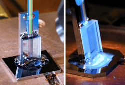
Researchers at the National Institute of Standard (NIST) Physical Measurement Lab (PML; Gaithersburg, MD) developed a small, robust chip-based photonic thermometer, and in the process, came up with what they say is a simple multifiber-to-chip alignment method of general utility.
When fully developed, the photonic thermometers could be used for remote thermometry, such as being buried into walls or sent into space; they could even be adapted for chemical, pressure, and humidity detection.
The PML researchers can simultaneously connect multiple optical fibers to a chip stably, cheaply, and rapidly, which could substantially speed up deployment of chip-scale photonic devices and standards by making possible high-volume manufacturing. For immediate purposes, the innovation means that these chip-based sensors are no longer effectively confined to a lab bench: they can now be easily transformed into portable thermometers and submitted to a wider range of tests.
Optical fibers carry light from source to chip and from chip to detector. But for fast testing of multiple devices, the team had always used a lab setup in which the fibers were suspended about a micrometer above the chip. This gap was small enough that the light was evanescently coupled with little loss.
Attaching individual fibers to chip structures one by one would have been tedious and time-consuming, says PML's Nikolai Klimov, who was tasked with addressing this challenge. To connect multiple fibers at a time, he considered a method that involves bonding an array of optical fibers to the edge of a chip. But this technique would have required the extra steps of precisely cutting off the chip's edge and optically polishing it to ensure efficient coupling. Another downside would have been the somewhat fragile interconnection due to the comparatively small surface area connecting the fiber array to the side of the chip, which in this case is a mere 0.7 mm thick.
Instead, Klimov used a commercially available optical fiber array, which comes assembled in a block with a set spacing between adjacent fibers. He then designed and built a photonic chip with the same set spacing between the adjacent light-collecting photonic structures. Using a custom-built platform with six degrees of freedom, he aligned the fiber array with the light-collecting photonic structures on top of the chip and held it in place with a droplet of UV light-curable transparent epoxy.
Although their first package uses an array that contains only 4 optical fibers, the method could be scaled up as much as 12 times by using off-the-shelf arrays that contain as many as 48 optical fibers in a block.
They have tested the new photonic thermometer packages from 10 to 80 °C, and neither the epoxy nor the fiber-to-chip bond has shown any signs of degradation. In the next few weeks they will continue to evaluate the packaged thermometers at a wider range of temperatures, from -40 to 150 °C. Other adhesives could enable light-coupled photonic chips at cryogenic temperatures to 4 K.
Source: http://www.nist.gov/pml/div685/grp01/photonic-thermometers-20150428.cfm

