Electrically pumped quantum-dot near-IR microlaser on silicon has submilliamp threshold
Researchers from the Hong Kong University of Science and Technology (HKUST) and the University of California, Santa Barbara (UCSB) have created record-small electrically pumped microlasers epitaxially grown on industry-standard (001) silicon (Si) substrates.1 The devices operate in a whispering-gallery-mode microlaser with a radius of 5 to 50 μm, have a submilliamp threshold of 0.6 mA (for the 5-μm-radius version), emit in the near-infrared (near-IR; 1.3 μm), and operate at temperatures up to 100°C. The thresholds and footprints are orders of magnitude smaller than previously reported lasers epitaxially grown on Si, the researchers say. Such lasers will be useful in the upcoming generation of silicon photonic circuits for communications and data centers.
It should be noted that a development similar in some ways was reported in 2016 by a group of researchers from University College London (London, England), the University of Sheffield (Sheffield, England), and Cardiff University (Cardiff, Wales), although these lasers did not operate in the whispering-gallery mode and were also much larger (3 mm long).2
III-V devices
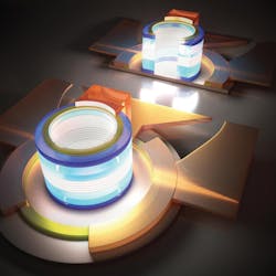
The gallium arsenide (GaAs)-based III-V semiconductor devices from HKUST and UCSB, which also incorporate aluminum (Al) and indium (In), consist of a GaAs layer on Si, 15 periods of thin (5 nm/5 nm) AlGaAs/GaAs layers, and seven InAs/InGaAs quantum dot-in-a-well layers in the laser's active region (see figure).
The 50-μm-radius whispering-gallery microresonator has a ring width of 5 μm and a calculated free-spectral range (FSR) of 1.56 μm. The measured FSR of the resonator was about 1.4 nm, agreeing well with the computer model. At an injection current of 80 mA, the output spectrum of the laser contains several individual lines between 1285 and 1300 nm, with the strongest line at 1294 nm. The version with a 50-μm-radius resonator produces a single laser line at about 1285 nm for injection currents between 0.6 and 1 mA.
The 50-μm-radius laser was subjected to high-temperature testing up to 100°C, which was as high as the test thermoelectric heater could go. The laser's slope efficiency decreased by 45% and 69% for pulsed and continuous-wave (CW) operation, respectively, when the heat-sink temperature increased from 10° to 100°C. The researchers note that the extraction of heat from the laser's active region could be optimized, and thus the temperature sensitivity reduced, by p-doping modulation of the active regions of the QDs.
"The realization of high-performance micron-sized lasers directly grown on Si represents a major step toward utilization of direct III-V/Si epitaxy as an alternate option to wafer-bonding techniques as on-chip silicon light sources with dense integration and low power consumption," says Kei May Lau, a professor at HKUST.
From optical to electrical pumping
The two groups had previously developed optically pumped CW microlasers operating at room temperature that were epitaxially grown on silicon with no germanium buffer layer or substrate miscut. "Electrical injection of microlasers is a much more challenging and daunting task: first, electrode metallization is limited by the micro-sized cavity, which may increase the device resistance and thermal impedance; second, the whispering gallery mode (WGM) is sensitive to any process imperfection, which may increase the optical loss," says Yating Wan, a HKUST PhD graduate who is now at UCSB.
"As a promising integration platform, silicon photonics needs on-chip laser sources that dramatically improve capability while trimming size and power dissipation in a cost-effective way for volume manufacturability," says John Bowers, deputy chief executive officer of AIM Photonics (Rochester, NY), a consortium devoted to developing the U.S integrated photonics industry. "The realization of high-performance micron-sized lasers directly grown on Si represents a major step toward utilization of direct III-V/Si epitaxy as an alternate option to wafer-bonding techniques.
REFERENCES
1. Y. Wan et al., Optica (2017); https://doi.org/10.1364/optica.4.000940.
2. S. Chen et al., Nature Photon. (2016); https://goo.gl/6XYfwJ.
About the Author

John Wallace
Senior Technical Editor (1998-2022)
John Wallace was with Laser Focus World for nearly 25 years, retiring in late June 2022. He obtained a bachelor's degree in mechanical engineering and physics at Rutgers University and a master's in optical engineering at the University of Rochester. Before becoming an editor, John worked as an engineer at RCA, Exxon, Eastman Kodak, and GCA Corporation.